Profiled high conductivity copper-tungsten electrical contact material and processing technique thereof

An electrical contact material, copper-tungsten alloy technology, applied in circuits, electrical switches, electrical components, etc., can solve the problems of reducing the connection strength of the weld, reducing the strength and elasticity of the copper, and the interface cannot be welded, so as to solve the problem of forming Difficulty, Elimination of Dispersibility, Conductivity and Improvement of Current Intermittent Characteristics

Inactive Publication Date: 2009-11-04
刘爱芬
View PDF0 Cites 8 Cited by
  • Summary
  • Abstract
  • Description
  • Claims
  • Application Information

AI Technical Summary

Problems solved by technology

[0004] At present, the following methods are mainly used in the production of copper-tungsten alloy integral parts at home and abroad: brazing, electron beam welding, hot isostatic pressure diffusion connection, etc. These methods have their own advantages and disadvantages. Experiments have proved that tungsten is very easy to absorb gas during welding. It will cause defects such as weld slag inclusions and pores, which will reduce the connection strength of the weld
At the same time, due to the thermal influence during the welding process, the copper material near the weld is in an annealed and softened state, which reduces the strength and elasticity of copper. In addition, the interface shape must be simple during welding, and complex interfaces cannot be welded
The hot isostatic pressing process has a large investment, and the process is very complicated and the consistency is not high
In addition, the overall copper-tungsten alloy material can also be used to process into special-shaped contacts, which has high processing costs, long processing time, and serious waste of materials.

Method used


Image

  • Profiled high conductivity copper-tungsten electrical contact material and processing technique thereof
  • Profiled high conductivity copper-tungsten electrical contact material and processing technique thereof

Examples


Embodiment Construction

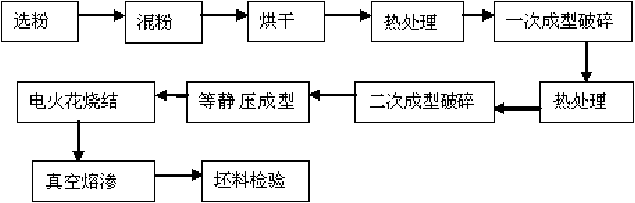
[0022] From figure 1 It can be seen from the figure that the processing process of special-shaped high-conductivity copper-tungsten alloy electrical contact materials is as follows:

[0023] First pass the copper powder through a 400-mesh sieve, select 3--6μm tungsten powder and mix it in a ratio of 0.3-0.8:99.7-99.2 by weight

[0024] Heat-treat the mixed raw material powder at a temperature of 580--620°C for 2--4 hours, at a temperature of 4.5--8.5 tons / cm 2 The pressure molding, crushing; then heat treatment at 620--670 ℃ for 2--4 hours, at 6--8.5 tons / cm 2 The pressure molding, crushing; the third heat treatment at a temperature of 670--700 ℃ for 2--4 hours, at 6--8.5 tons / cm 2 The pressure molding, crushing; finally isostatic pressing into the required shape, and then electric spark sintering into a copper-tungsten alloy billet.

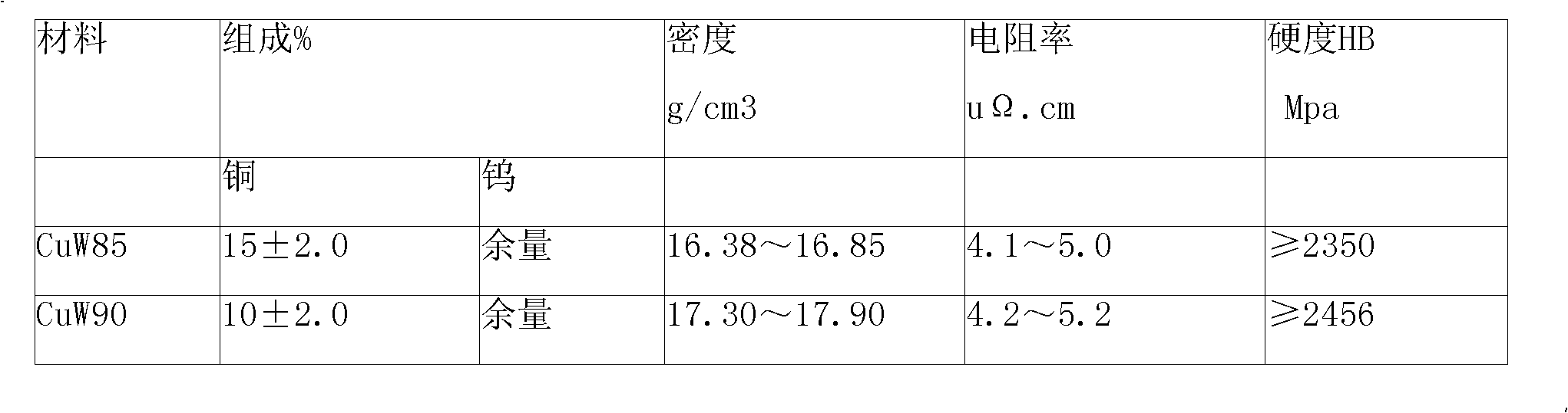
[0025] The prepared pure copper and the sintered billet are vacuum infiltrated to make the copper content reach 8--17%, and various shapes o...


PUM


Abstract

The invention discloses a profiled high conductivity copper-tungsten electrical contact material and a processing technique thereof. the processing technique is characterized by firstly choosing copper powder and tungsten powder with suitable granularity and mixing the powders according to a certain proportion; carrying out to-and-fro heat treatment, press forming and smashing on the mixed raw powder, then isostatically pressing a required shape and sintering the shape with electric sparks into copper tungsten blanks; lastly, carrying out vacuum infiltration on the prepared copper and the sintered blanks to ensure that copper can be totally infiltrated into the body during material production to produce the profiled high conductivity copper-tungsten electrical contact material with the porosity of less than 0.15%. The electrical contact produced by the contact material simplifies construction of electric switches, eliminates the dispersivity of the springs in the switches and greatly improves the reliability of components. The material is widely used in high temperature materials, electrical alloys for high voltage switches, electromachining electrodes, microelectronic materials and the like.

Description

technical field [0001] The invention relates to an electrical contact material in a vacuum circuit breaker, in particular to a high-power silver-free copper-tungsten alloy contact material and its processing technology. Background technique [0002] Copper-tungsten alloy is a two-phase structure pseudo-alloy mainly composed of copper and tungsten elements. It is a metal matrix composite material. The alloy has the characteristics of high temperature resistance, arc ablation resistance, high strength, high specific gravity, good electrical and thermal conductivity, etc. This product is widely used in high temperature resistant materials, electrical alloys for high voltage switches, electrical processing electrodes, microelectronic materials, etc. Parts and components are widely used in aerospace, aviation, electronics, electric power, metallurgy and other industries. [0003] Due to the large difference in physical properties between metal copper and tungsten, it cannot be p...

Claims


Application Information

Patent Timeline
Patent Type & Authority Applications(China)
IPC IPC(8): H01H11/04B22F3/16
Inventor 宋和明
Owner 刘爱芬
Why Eureka
Try Eureka