
Devices and methods for pattern generation by ink lithography

A device and pattern technology, applied in the photoengraving process, instruments, optics and other directions of the pattern surface, can solve the problems such as hindering the high-yield manufacturing of micro-scale and nano-scale devices, distortion of relief patterns, and being unsuitable for patterning. Improved overall efficiency and energy consumption, enhanced fidelity effects

Inactive Publication Date: 2009-11-04
THE BOARD OF TRUSTEES OF THE UNIV OF ILLINOIS
View PDF2 Cites 32 Cited by
  • Summary
  • Abstract
  • Description
  • Claims
  • Application Information

AI Technical Summary

Problems solved by technology

While nanolithography offers viable methods for fabricating nanoscale structures and devices, these methods have certain limitations that prevent their practical integration into commercial methods that can provide low-cost, high-volume processing of nanomaterials
First, nanolithography methods require elaborate and expensive steppers or writing tools to direct light, electrons and / or ions onto the photoresist surface
Second, these methods are limited to patterning a very narrow range of specialized materials and are not suitable for introducing specific chemical functionalities into nanostructures
Third, conventional nanolithography is limited to the fabrication of nanoscale features on small areas of ultra-flat rigid surfaces, making them less suitable for patterning glass, carbon, and plastic surfaces
[0013] While the use of conventional composite templates and molds has somewhat improved the performance of soft lithography methods for generating features with dimensions in the sub-100nm range, these techniques are still susceptible to several issues that prevent their Efficient commercial application for high-throughput fabrication of microscale and nanoscale devices
First, some conventional template and mold designs have limited flexibility such that good conformal contact with distorted or rough surfaces is not possible
Second, the relief pattern of conventional multi-material PDMS templates is susceptible to unwanted shrinkage during thermal or UV curing, which distorts the relief pattern on the transfer surface of this template
Third, the use of conventional composite templates comprising multiple layers with different coefficients of thermal expansion can lead to distortion of the relief pattern and curvature of the transfer surface of the template due to temperature changes
Fourth, the use of hard and / or brittle backing layers, such as glass and certain metal layers, makes conventional composite stencils difficult to incorporate into existing commercial printing configurations, such as roll and flexo press configurations
Especially after complex processes on plastic substrates, unexpected misfits due to thermal expansion or residual tension make precise alignment impossible

Method used


Image

  • Devices and methods for pattern generation by ink lithography
  • Devices and methods for pattern generation by ink lithography
  • Devices and methods for pattern generation by ink lithography

Examples


Embodiment 1

[0185] Embodiment 1: Composite template for nano transfer printing

[0186] Experimental studies validate the ability of the composite patterned devices of the present invention to provide composite templates for nanotransfer printing applications. In particular, it is an object of the present invention to provide composite templates capable of patterning large areas of substrate surfaces with structures of selected lengths on the order of micrometers and tens of nanometers. Furthermore, it is an object of the present invention to provide composite templates for contact printing high resolution patterns exhibiting good fidelity and layout accuracy.

[0187] In order to achieve the aforementioned goals, composite templates were fabricated using the method of the present invention and used to generate patterns comprising gold monolayers on substrates via nanotransfer printing (nTP). Specifically, a polyimide containing 25 µm thick ( Large-area composite templates of thin (5...

Embodiment 2

[0195] Example 2: Computer Modeling of Thermal and Mechanical Properties of Composite Patterned Devices

[0196] Computational simulations evaluated the susceptibility of the inventive multilayer patterned devices to distortions caused by mechanical stress and aggregation during fabrication. Specifically, the degree of deformation induced by aggregation during fabrication and gravity-induced deformation of the recessed regions was calculated for a four-layer composite patterned device. These studies demonstrate that the composite patterned devices of the present invention exhibit enhanced stability against polymerization-induced shrinkage and gravity-induced bowing.

[0197] Calculate and compare the degree of distortion caused by aggregation for two different composite template designs. first, Figure 10 A schematically shown four-layer composite patterned device 600 comprising a 5 micron thick first PDMS polymer layer 610, a 25 micron thick second polyimide Polymer lay...

Embodiment 3

[0201] Example 3: Fiber-reinforced composite patterned device

[0202] The present invention includes composite patterned devices comprising one or more composite polymer layers, including polymer layers having fibrous materials that provide beneficial mechanical, structural, and / or thermal properties. Composite patterned devices of this aspect of the invention include designs in which fibers are integrated into and / or between polymer layers in selected geometries - the geometries are selected to provide a relief feature that embosses the pattern. Distortion-minimized net flexural stiffness provides the ability to generate patterned devices exhibiting good fidelity and layout accuracy on the substrate surface. Furthermore, the composite patterned devices of this aspect of the invention include designs in which fibers are integrated into and / or between polymer layers in selected geometries such that expansion and Shrinkage is minimized, and / or facilitated for practical manip...


PUM

PropertyMeasurementUnit
Thicknessaaaaaaaaaa

Abstract

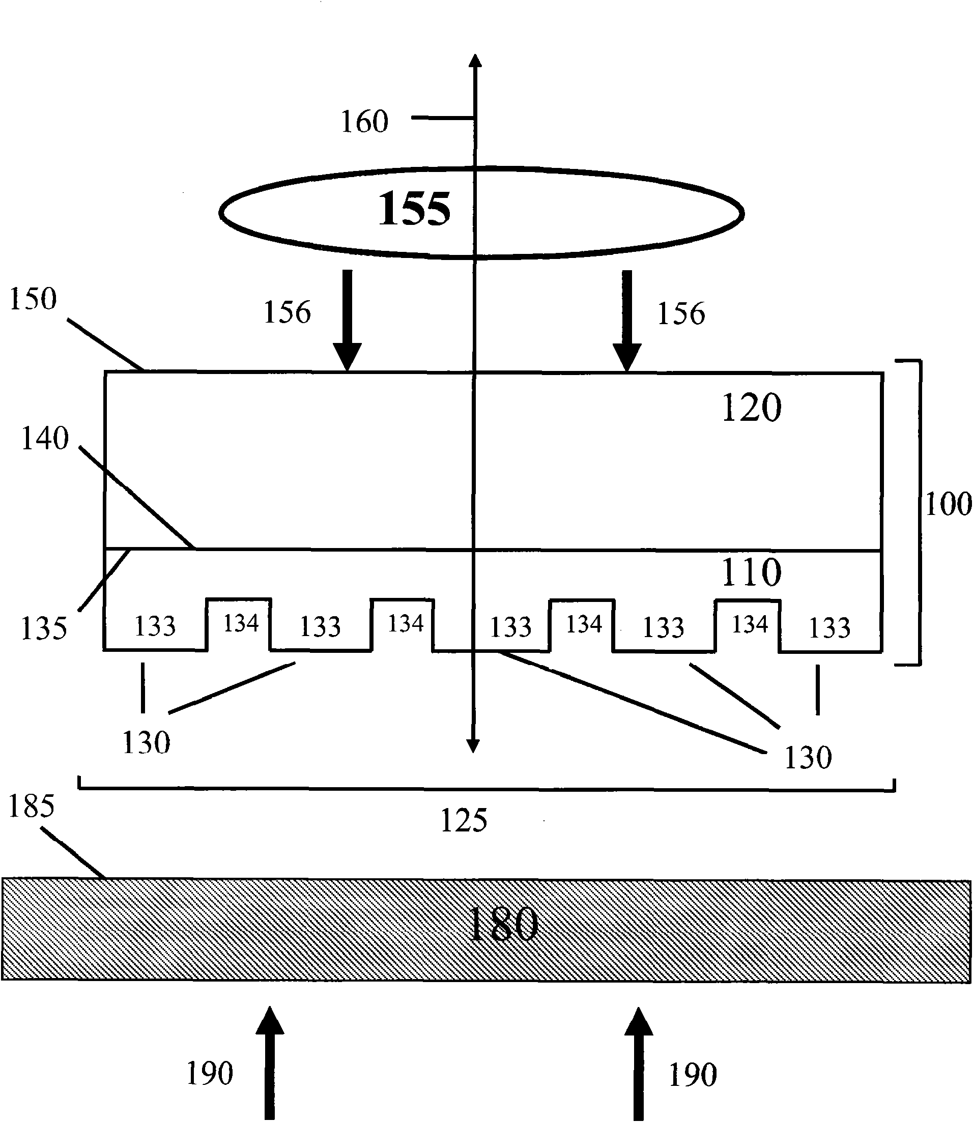
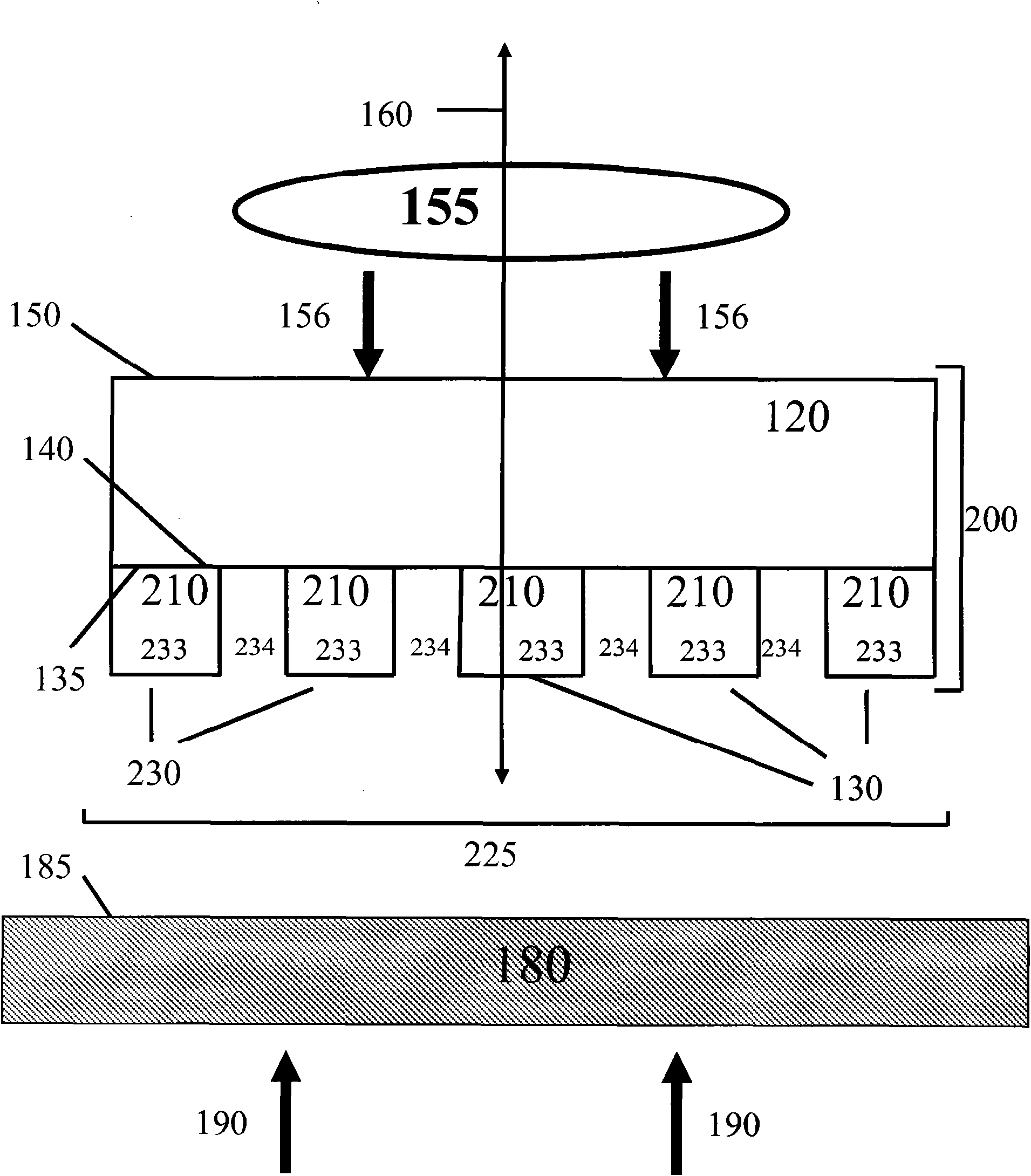
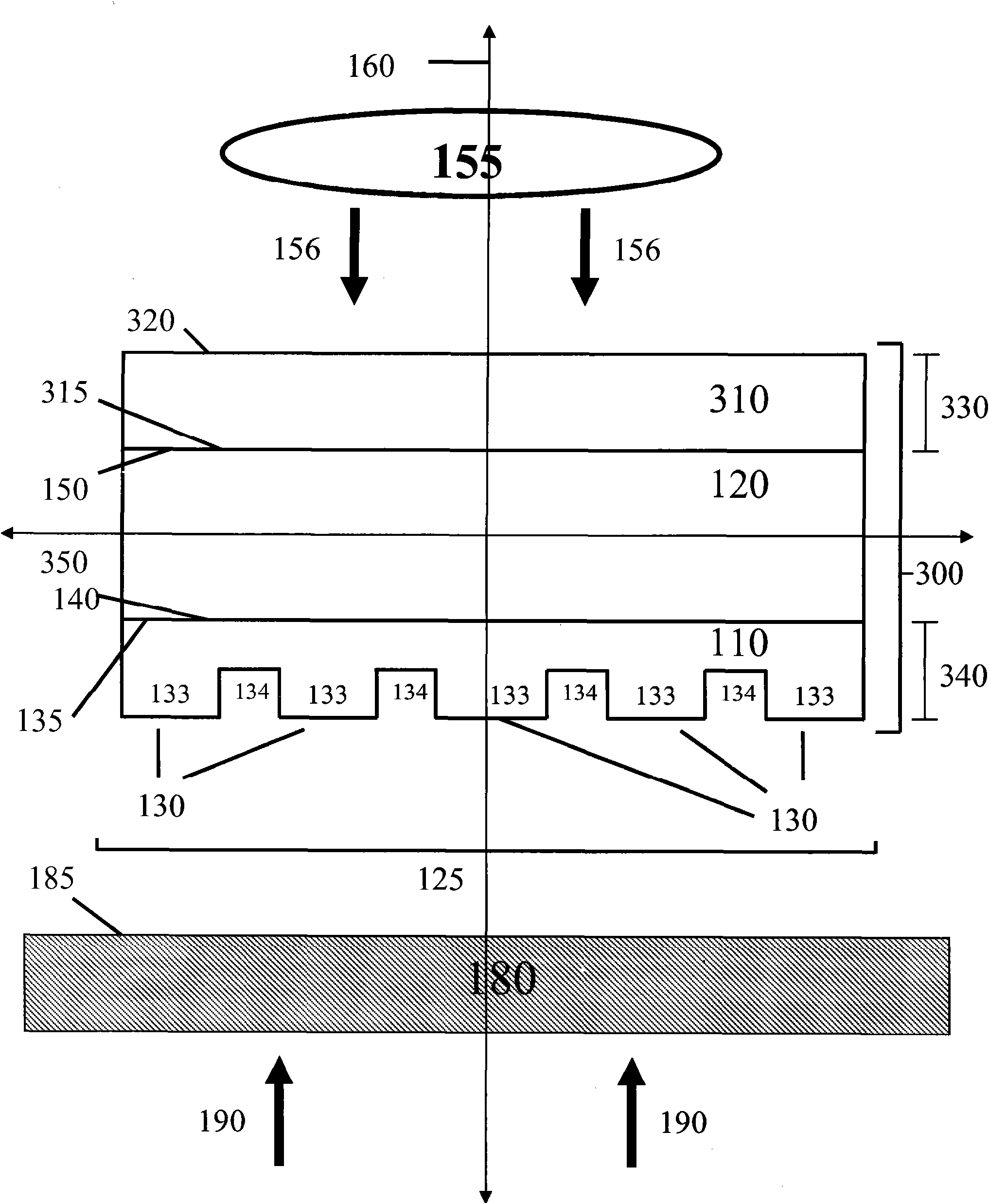
The present invention provides methods, devices and device components for fabricating patterns on substrate surfaces, particularly patterns comprising structures having microsized and / or nanosized features of selected lengths in one, two or three dimensions and including relief and recess features with variable height, depth or height and depth. Composite patterning devices comprising a plurality of polymer layers each having selected mechanical and thermal properties and physical dimensions provide high resolution patterning on a variety of substrate surfaces and surface morphologies. Gray-scale ink lithography photomasks for gray-scale pattern generation or molds for generating embossed relief features on a substrate surface are provided. The particular shape of the fabricated patterned can be manipulated by varying the three-dimensional recess pattern on an elastomeric patterning device which is brought into conformal contact with a substrate to localize patterning agent to the recess portion of the pattern.

Description

[0001] Cross References to Related Applications [0002] This application claims the benefit of US Provisional Patent Application 60 / 863,248, filed October 27, 2006, and US Nonprovisional Patent Application 11 / 675,659, filed February 16, 2007, both of which are incorporated herein by reference in their entirety. Background of the invention [0003] The design and fabrication of micron-scale structures and devices has enormous implications for a variety of important technologies, including microelectronics, optoelectronics, microfluidics, and microsensing. For example, the ability to fabricate micron-sized electronic devices has revolutionized the field of electronics, resulting in faster and higher performing electronic components with significantly less energy requirements. As these technologies continue to advance at a rapid pace, it has become increasingly apparent that further gains will be realized by developing the ability to manipulate and organize matter at the nanosca...

Claims


Application Information

Patent Timeline
IPC IPC(8): G03F9/00G03F7/00G03B27/04
Inventor J·A·罗杰斯E·梅纳德
Owner THE BOARD OF TRUSTEES OF THE UNIV OF ILLINOIS
Learn More