

Double-layer anti-reflecting film of crystal silicon solar cell and preparation method thereof
A solar cell and anti-reflection film technology, applied in the field of solar cells, can solve the problems of limited photoelectric conversion efficiency, low refractive index, and poor reflection effect, and achieve low cost, low deposition temperature, and good anti-reflection effect
- Summary
- Abstract
- Description
- Claims
- Application Information
AI Technical Summary
Problems solved by technology
Method used
Image

Examples
Embodiment 1
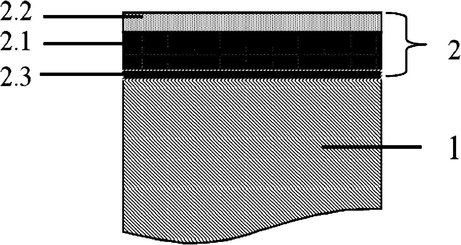
[0037] On the silicon-based substrate 1 surface, utilize the magnetron sputtering deposition method, the metal Ti target is the sputtering target, argon (Ar):oxygen (O 2 ) The gas flow ratio is 1-10, the sputtering pressure is 0.5Pa-2Pa, the sputtering power is 250W-350W, and a layer of TiO 2 The dense layer 2.1 has a thickness of 40-60 nm, and its refractive index at 600 nm wavelength is 2.7-2.9. Sputtering power changed to 100W ~ 200W, in TiO 2 Prepare a layer of TiO on the dense layer 2.1 2 The thickness of the loose layer 2.2 is controlled to be 60-80 nm, and the refractive index of the layer is 1.9-2.1 at a wavelength of 600 nm. Deposited quasi-bilayer TiO 2 The silicon substrate of the anti-reflection film, after being printed with electrode silver paste, undergoes conventional sintering at 400°C to 900°C, and the silicon substrate and dense TiO 2 SiO with a thickness of 1nm to 20nm is formed at the interface 2 passivation layer.
Embodiment 2
[0039] On the surface of the silicon-based substrate 1, the atmospheric pressure chemical vapor deposition method is used to form Ti(OC 3 h 7 ) 4 as the source material, Ti(OC 3 h 7 ) 4 The volume fraction is 0.5-2%; 2 It is the reaction gas, the volume fraction is 0.5~2%; as N 2 Gas is the carrying gas, the volume fraction is the balance, the deposition temperature is 500-700°C, and the holding time is 0.5 hours. The prepared TiO 2 The thickness of the dense layer is 40-60nm, and its refractive index at 600nm wavelength is 2.7-2.9. The deposition temperature is changed to 350-450°C, and the TiO 2 Prepare a layer of TiO on the dense layer 2.1 2 The thickness of the loose layer 2.2 is controlled to be 60-80 nm, and the refractive index of the layer at a wavelength of 600 nm is 1.9-2.1. Deposited quasi-bilayer TiO 2 The silicon substrate, after printing with electrode silver paste, undergoes conventional sintering at 400°C to 900°C, and the silicon substrate and dense ...
Embodiment 3
[0041] On the surface of the silicon-based substrate 1, using the plasma chemical vapor deposition method, Ti(OC 3 h 7 ) 4 as the source material, Ti(OC 3 h 7 ) 4 The volume fraction is 0.5-2%, with O 2 It is the reaction gas, the volume fraction is 0.5~2%; as N 2 Gas is the carrying gas, the volume fraction is the balance, and the deposition temperature is 500-700°C to prepare TiO 2 The thickness of the dense layer is 40-60nm, and its refractive index at 600nm wavelength is 2.7-2.9. The deposition temperature was changed to 300-400°C, and the TiO 2 Prepare a layer of TiO on the dense layer 2.1 2 The thickness of the loose layer 2.2 is controlled to be 60-80 nm, and the refractive index of the layer is 1.9-2.1 at a wavelength of 600 nm. Deposited quasi-bilayer TiO 2 After the silicon substrate is printed with electrode silver paste, it is conventionally sintered at 400°C to 900°C, and the silicon substrate and the dense layer of TiO 2 SiO with a thickness of 1nm to ...
PUM
| Property | Measurement | Unit |
|---|---|---|
| Thickness | aaaaa | aaaaa |
| Thickness | aaaaa | aaaaa |
| Thickness | aaaaa | aaaaa |
Abstract
Description
Claims
Application Information