Low-resistance high-transmittance shielding film for plasma displays
A plasma display and shielding film technology, applied in optics, instruments, optical components, etc., can solve the problems of bonding conductive bus bar loss, system error, etc., to achieve protection from erosion, tight structure, enhanced light transmission and conductivity. Effect
- Summary
- Abstract
- Description
- Claims
- Application Information
AI Technical Summary
Problems solved by technology
Method used
Image
Examples
Embodiment Construction
[0025] Below in conjunction with accompanying drawing, the present invention is described in further detail:
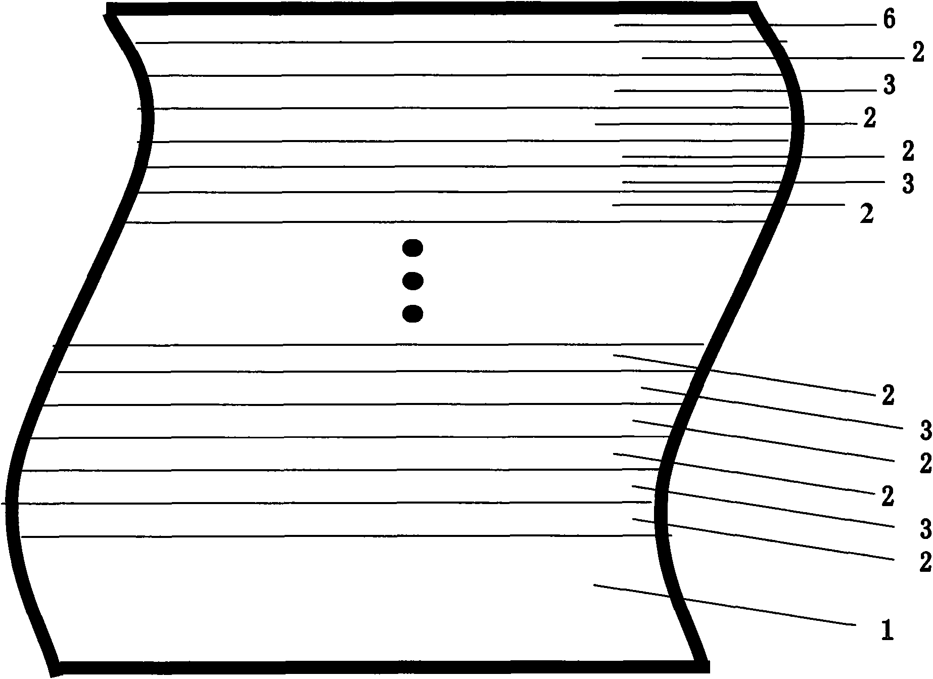
[0026] like figure 1 As shown, the low-resistance and high-transparency shielding film of plasma display of the present invention comprises a bottom layer, an intermediate layer and a surface layer; wherein the bottom layer is a flexible organic base material layer; 2 layer, Ag layer, TiO 2 layer, repeated n times, n is a natural number, and n≥3; the surface layer is an ITO layer;
[0027] In addition, the organic base material layer, TiO 2 layer, Ag layer and ITO layer are honeycomb composite structure on the surface, TiO 2 layer and ITO layer can be directly sputtered with a ceramic target, and the thickness is between 10nm and 50nm. Ag layer thickness between 12nm and 20nm, TiO 2 layer and the thickness of the ITO layer is between 10nm and 50nm. Because TiO 2 The surface of Ag layer / Ag layer / ITO layer (D / M / D for short) structure needs to form a honeycomb str...
PUM
 Abstract
Description
Claims
Application Information
 - R&D
- Intellectual Property
- Life Sciences
- Materials
- Tech Scout
- Unparalleled Data Quality
- Higher Quality Content
- 60% Fewer Hallucinations
Browse by: Latest US Patents, China's latest patents, Technical Efficacy Thesaurus, Application Domain, Technology Topic, Popular Technical Reports.
© 2025 PatSnap. All rights reserved.Legal|Privacy policy|Modern Slavery Act Transparency Statement|Sitemap|About US| Contact US: help@patsnap.com


