Doping modified phase change material and phase change storage unit containing same and preparation method thereof

A technology of phase-change memory and phase-change materials, which is applied in the field of micro-nano electronics, can solve problems such as failure to meet practical application requirements, poor chip data retention, and low crystallization temperature, and achieve the goal of overcoming poor data retention, low power consumption, The effect of low melting point

Active Publication Date: 2009-11-18
SHANGHAI INST OF MICROSYSTEM & INFORMATION TECH CHINESE ACAD OF SCI
View PDF0 Cites 40 Cited by
  • Summary
  • Abstract
  • Description
  • Claims
  • Application Information

AI Technical Summary

Problems solved by technology

[0005] Sb 2 Se 3 Storage materials have the advantages of fast phase change speed and low melting point, and have good application prospects in high-speed, low-power phase-change memory, but Sb 2 Se 3 The disadvantage of storage materials is that the crystallization temperature is low. After being used in phase change memory, the data retention of the chip is poor, which cannot meet the requirements of practical applications.

Method used


Image

  • Doping modified phase change material and phase change storage unit containing same and preparation method thereof
  • Doping modified phase change material and phase change storage unit containing same and preparation method thereof
  • Doping modified phase change material and phase change storage unit containing same and preparation method thereof

Examples


Embodiment 1

[0033] The present invention contains (Sb 2 Se 3 ) 100-x Y x The preparation process of the phase change memory device unit of the phase change material is as follows:

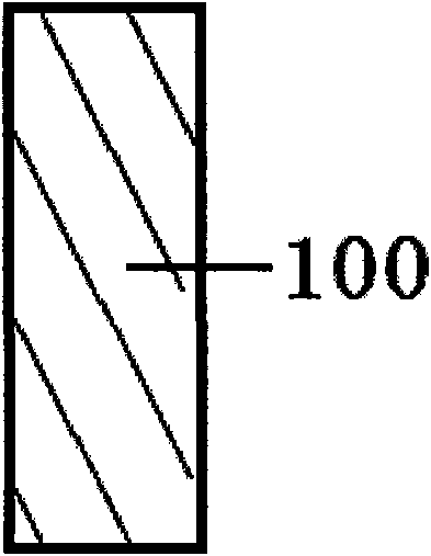
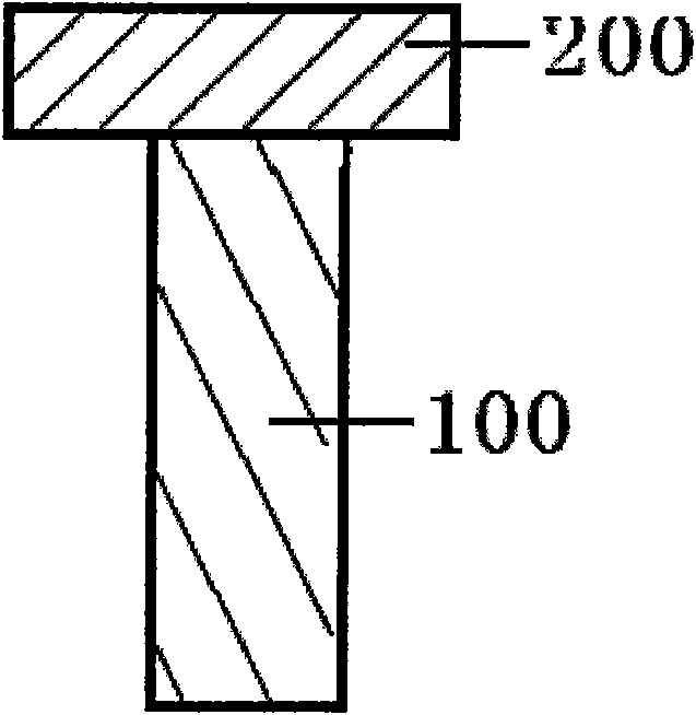
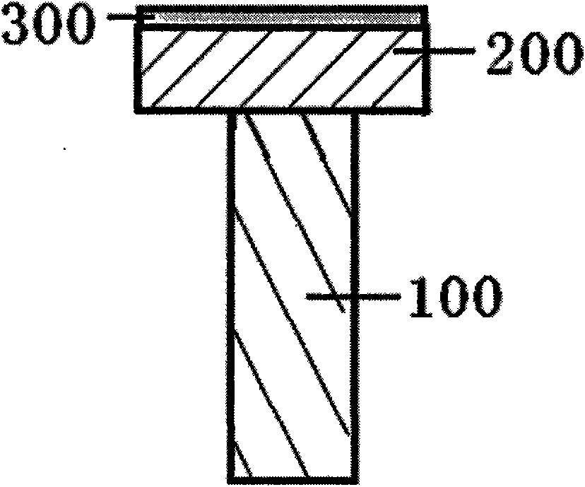
[0034] Step 1: See figure 1, using sputtering, evaporation, chemical vapor deposition (CVD), plasma enhanced chemical vapor deposition (PECVD), low pressure chemical vapor deposition (LPCVD), metal compound vapor deposition (MOCVD), molecular beam epitaxy The lower electrode layer 100 is prepared by any one of (MBE), atomic vapor deposition (AVD) or atomic layer deposition (ALD). In this embodiment, the lower electrode layer 100 is preferably prepared by CVD. The material of the lower electrode layer 100 is one of the single metal materials W, Pt, Au, Ti, Al, Ag, Cu or Ni, or an alloy material composed of any two or more of the single metal materials, or The nitride or oxide of the single metal material is preferably W in this embodiment. The resulting W electrode had a diameter of 80 nm and a height of...

Embodiment 2

[0042] The same technical solution as in the first embodiment is adopted, except that the preparation method of the phase-change material layer 300 is changed to AVD or ALD, and the rest of the steps are exactly the same as in the first embodiment, and the same technical effect can also be achieved.

Embodiment 3

[0044] Adopt the same technical scheme as embodiment one or two, the difference is that the phase change material in embodiment one or two is changed into (Sb 2 Se 3 ) 92 N 8 . where for Sb 2 Se 3 The element for material doping is any one of C, N or O, preferably N here. The doping of N adopts the reactive magnetron sputtering method, and the process parameters are: the background pressure is 1×10 -5 Pa, the gas pressure during sputtering is 0.3Pa, Ar / N 2 The ratio of the gas flow rate is 25:1, the sputtering power is 500W, and the substrate temperature is 25°C.


PUM

PropertyMeasurementUnit
diameteraaaaaaaaaa
heightaaaaaaaaaa
thicknessaaaaaaaaaa

Abstract

The invention relates to a doping modified phase change material and a phase change storage unit containing same and preparation thereof. The formula of the doping modified phase change material is (Sb2Se3)100-xYx, wherein, x is the atom percentage of an element and is more than 0 and less than or equal to 20, and Y is a doped element and is any one of Ni, Cr, Bi, As, Ga, In, Ge, Si, Sn, Ag, Al, C, N and O. The doping modified (Sb2Se3)100-xYx storage material not only remains the advantages of the fast phase change speed and the low melting point of Sb2Se3 storage material, but also increases crystallization temperature, thus overcoming the disadvantage of poor data retentivity of the Sb2Se3 storage material. The phase change storage containing the (Sb2Se3)100-xYx storage material has the advantages of high speed, low power consumption and favorable data retentivity and the like.

Description

technical field [0001] The invention relates to a phase change material, a phase change memory device unit containing the material and a preparation method thereof, in particular to a phase change that can improve the programming speed of the phase change memory, reduce the programming power consumption of the device, and improve the data retention of the device Material, phase change memory device unit containing the material and its preparation method. The invention belongs to the technical field of micro-nano electronics. Background technique [0002] Phase-change memory technology is based on the idea that phase-change thin films can be applied to phase-change storage media proposed by Ovshinsky in the late 1960s and early 1970s. It is a storage device with low price and stable performance. Phase-change memory can be made on a silicon wafer substrate, and its key materials are recordable phase-change films, heating electrode materials, heat insulating materials, and lea...

Claims


Application Information

Patent Timeline
Patent Type & Authority Applications(China)
IPC IPC(8): H01L45/00G11C11/56
Inventor 刘波宋志棠张挺封松林
Owner SHANGHAI INST OF MICROSYSTEM & INFORMATION TECH CHINESE ACAD OF SCI
Why Eureka
Try Eureka