

Detection method for evaluating group III nitride single crystal surface dislocation
A detection method and nitride technology, applied in surface/boundary effects, measurement devices, preparation of test samples, etc., can solve problems such as inability to distinguish dislocation types, long period, pollution, etc., to improve performance evaluation efficiency, promote The effect of further development and accurate determination
- Summary
- Abstract
- Description
- Claims
- Application Information
AI Technical Summary
Problems solved by technology
Method used
Image

Examples
Embodiment 1
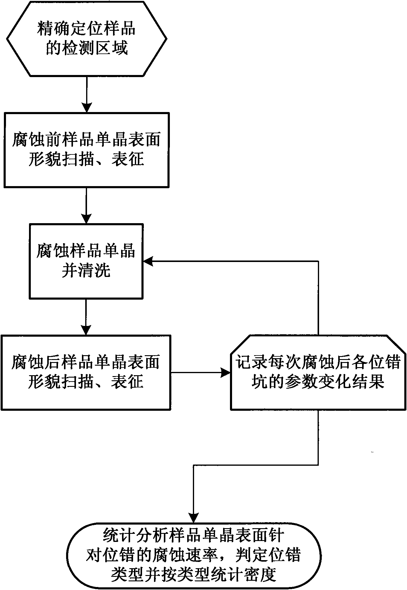
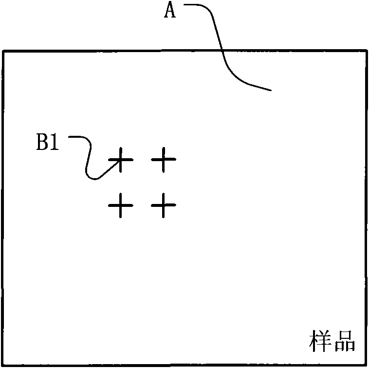
[0027] The first step—precise positioning of the detection area: use the diamond probe of the nanoindenter to mark four crosses B1 (such as Figure 2a As shown), a square detection area with an area of about 50×50 μm is formed, the length of the scribed line is about 2 μm, the width of the scratch is about 1 μm, and the depth is 2 μm.
[0028] The second step—scanning and characterization of the original surface morphology of the sample before corrosion: use the optical microscope configured by the atomic force microscope to locate the center of the detection area drawn by the nanoindentation instrument, and scan the area from large to small 50×50 μm, 20× Topography of 20μm, 10×10μm, 5×5μm, 2×2μm, selected as image 3 The square shown is used as the colocation test area, and the total number of dislocations in this area can be obtained as follows: image 3 15 are shown, and the area of the dislocation pit with the symbol 1 is the largest, about 70.8nm 2 , and the area of...
Embodiment 2
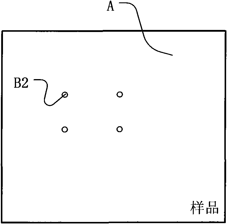
[0035] The detection method of the present invention may also have other implementation modes, which are embodied in the precise positioning detection area mode in step 1. That is, four dots B2 (such as Figure 2b As shown), a square detection area with an area of about 50×50 μm is formed, and the diameter of the etched dot is about 1 μm. Subsequent steps in this embodiment are the same as those in Embodiment 1, so details are not repeated here.
[0036] According to the steps of the above-mentioned embodiment, by wet etching the single crystal surface of the III-nitride sample combined with the co-situ observation of the atomic force microscope, the accurate determination of the dislocation type on the single crystal surface is realized, and the performance evaluation efficiency of the III-nitride-based optoelectronic device is improved. This further promotes the further development of this material in optoelectronic industries such as light-emitting diodes, and also provi...
PUM
| Property | Measurement | Unit |
|---|---|---|
| electrical resistivity | aaaaa | aaaaa |
Abstract
Description
Claims
Application Information