Multilayer transparent electricity conductive film and manufacture method

A transparent conductive film and thin film technology, applied in cable/conductor manufacturing, chemical instruments and methods, conductive layers on insulating carriers, etc. The effect of industrial production and simple method

Inactive Publication Date: 2009-12-23
ZHEJIANG UNIV
View PDF0 Cites 38 Cited by
  • Summary
  • Abstract
  • Description
  • Claims
  • Application Information

AI Technical Summary

Problems solved by technology

At present, there are many studies on ZnO transparent conductive films, but the electrical properties of single-layer ZnO films obtained at room temperature are still difficult to compare with ITO
It is repo

Method used


Image

  • Multilayer transparent electricity conductive film and manufacture method
  • Multilayer transparent electricity conductive film and manufacture method
  • Multilayer transparent electricity conductive film and manufacture method

Examples


Embodiment 1

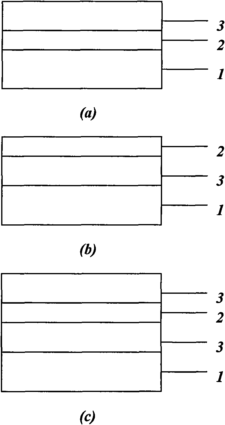
[0038] Embodiment 1: Cu / ZnO: the preparation method of Ga multilayer transparent conductive film

[0039] Clean the glass substrate and place it on the sample holder of the reaction chamber of the magnetron sputtering device. The substrate deposition surface is placed downwards, which can effectively prevent the contamination of the substrate surface by granular impurities. The vacuum degree of the reaction chamber is pumped to at least 3 ×10 -3 Pa, with Cu metal as the target material and pure Ar as the sputtering gas into the reaction chamber, the metal Cu layer was deposited by DC reactive magnetron sputtering. The gas pressure is 1.0Pa, the sputtering power is 120W, and the substrate temperature is normal temperature to carry out deposition and growth. The film thickness is determined by the growth time, monitored in real time by an oscillating film thickness monitor, and accurately measured by an ellipsometer. The deposition time is 0-20s, and the thickness of the metal...

Embodiment 2

[0044] Embodiment 2: ZnO: Ga / Cu / ZnO: the preparation method of Ga multilayer transparent conductive film

[0045] Clean the glass substrate and place it on the sample holder of the reaction chamber of the magnetron sputtering device. The substrate deposition surface is placed downwards, which can effectively prevent the contamination of the substrate surface by granular impurities. The vacuum degree of the reaction chamber is pumped to at least 3 ×10 -3 Pa, with a (Zn+Ga) alloy containing 4% Ga by mole percent as the target material, with pure Ar and pure O 2 As the sputtering gas was input into the reaction chamber, the transparent ZnO layer was deposited by DC reactive magnetron sputtering. Ar:O 2 =10:1, the gas pressure is 3.3Pa, the sputtering power is 140W, and the substrate temperature is normal temperature, and the deposition and growth are carried out. The thickness of the transparent ZnO layer is 30 nm.

[0046] After the first transparent ZnO layer is sputtered, ...

Embodiment 3

[0051] Embodiment 3: Cu (10nm) / ZnO:Ga (60nm) annealing

[0052] The Cu(10nm) / ZnO:Ga(60nm) multilayer transparent conductive film of structure obtained in embodiment 1 is annealed under vacuum environment, and annealing vacuum is 3 * 10 -3 Pa, the annealing time is 45 minutes, and the annealing temperature range is 200-600°C.

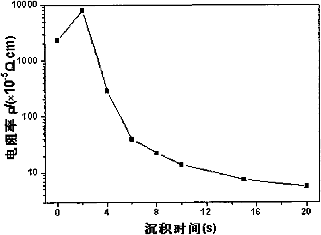
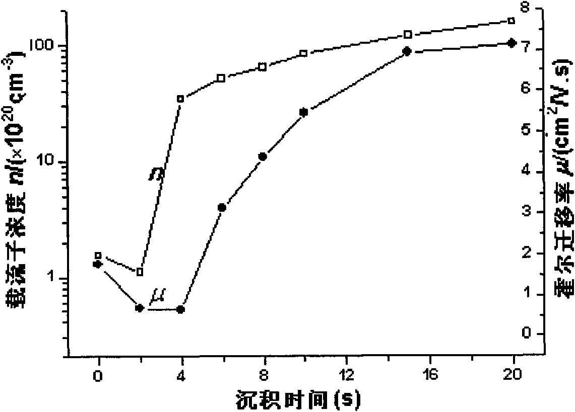
[0053] After annealing, the resistivity ρ and optical transmittance curves of Cu(10nm) / ZnO:Ga(60nm) structured multilayer transparent conductive film with annealing temperature are as follows: Figure 8 and 9 shown. Combining the light-transmitting and conductive properties of the multilayer transparent conductive film, the optimal annealing temperature is 400°C.

[0054] Cu(10nm) / ZnO:Ga(60nm) structured multi-layer transparent conductive film at 3×10 -3 After annealing at 400°C for 45 minutes in a vacuum environment of Pa, the photoelectric performance index of the thin film structure:

[0055] Resistivity


PUM

PropertyMeasurementUnit
Thicknessaaaaaaaaaa

Abstract

The invention provides a multilayer transparent electricity conductive film, comprising a substrate, n layers of metal Cu layers and m layers of ZnO layers. The n layers of metal Cu layers and the m layers of ZnO layers are alternately deposited on the substrate, wherein n is more than and equal to 1, and m is more than and equal to 1. The film is manufactured by a magnetic control sputtering method. The multilayer transparent electricity conductive film is characterized in that: the average transmittance of a visible light area is more than 70%, peak value transmittance is larger than 80%, the concentration of electron current carrier is not less than 5*10cm, and electric resistivity is not larger than 3*10 Omega. cm. The multilayer film obtained by the invention is manufactured under room temperature; the photoelectric property of the film is greatly improved relatively to a ZnO: Ca monolayer film; and the multilayer film can be used for photoelectric devices such as solar battery, flat-panel display, and the like, and the structure of a sunshade type infrared reflecting film.

Description

technical field [0001] The invention relates to a multi-layer transparent conductive film used for optoelectronic devices such as solar panels, flat panel displays, and devices such as sun-shading infrared reflection structures, and belongs to the field of optoelectronic information functional materials. Background technique [0002] As an important optoelectronic information material, transparent conductive oxide (TCO) thin films are widely used in solar cells, flat panel displays, light emitting devices, sensors, and electromagnetic shielding. Among such materials, zinc oxide (ZnO) is more important than indium tin oxide (ITO) and tin oxide (SnO 2 ), has the advantages of cheap, non-toxic, and good stability in the hydrogen plasma environment, and is one of the most promising materials to replace ITO. By doping Ga or Al, the conductivity of ZnO can be increased by three to five orders of magnitude. At present, there are many studies on ZnO transparent conductive films, b...

Claims


Application Information

Patent Timeline
IPC IPC(8): H01B5/14H01B13/00B32B9/04B32B15/04C23C14/35C23C14/08C23C14/18
Inventor 吕建国别勋叶志镇
Owner ZHEJIANG UNIV
Why Eureka
Try Eureka