
High-efficiency radiating LED illumination light source and manufacture method

A technology for LED lighting and a manufacturing method, which is applied in the manufacturing field of the high-efficiency heat-dissipating LED lighting source, can solve the problems of complex process, high cost, low production efficiency, etc., and achieves excellent thermal conductivity, reduced heat dissipation base, and high manufacturing process precision Effect

Inactive Publication Date: 2009-12-30
NANKER GUANGZHOU SEMICON MFG
View PDF0 Cites 25 Cited by
  • Summary
  • Abstract
  • Description
  • Claims
  • Application Information

AI Technical Summary

Problems solved by technology

The manufacturing process of this kind of integrated LED chip light source needs to first package the LED bare chip first, and then perform secondary packaging on the aluminum substrate with circuit, so the process is complicated, the cost is high, and the production efficiency is low.

Method used


Image

  • High-efficiency radiating LED illumination light source and manufacture method
  • High-efficiency radiating LED illumination light source and manufacture method
  • High-efficiency radiating LED illumination light source and manufacture method

Examples


Embodiment Construction

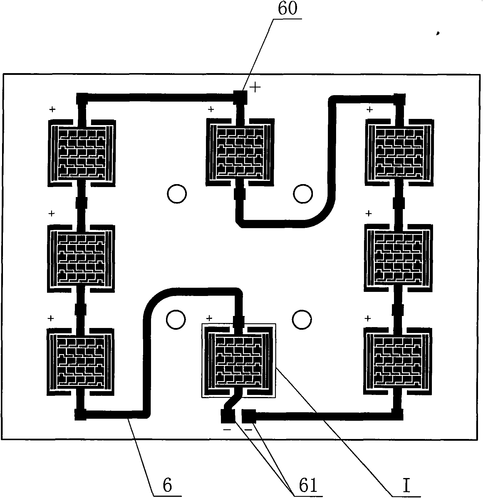
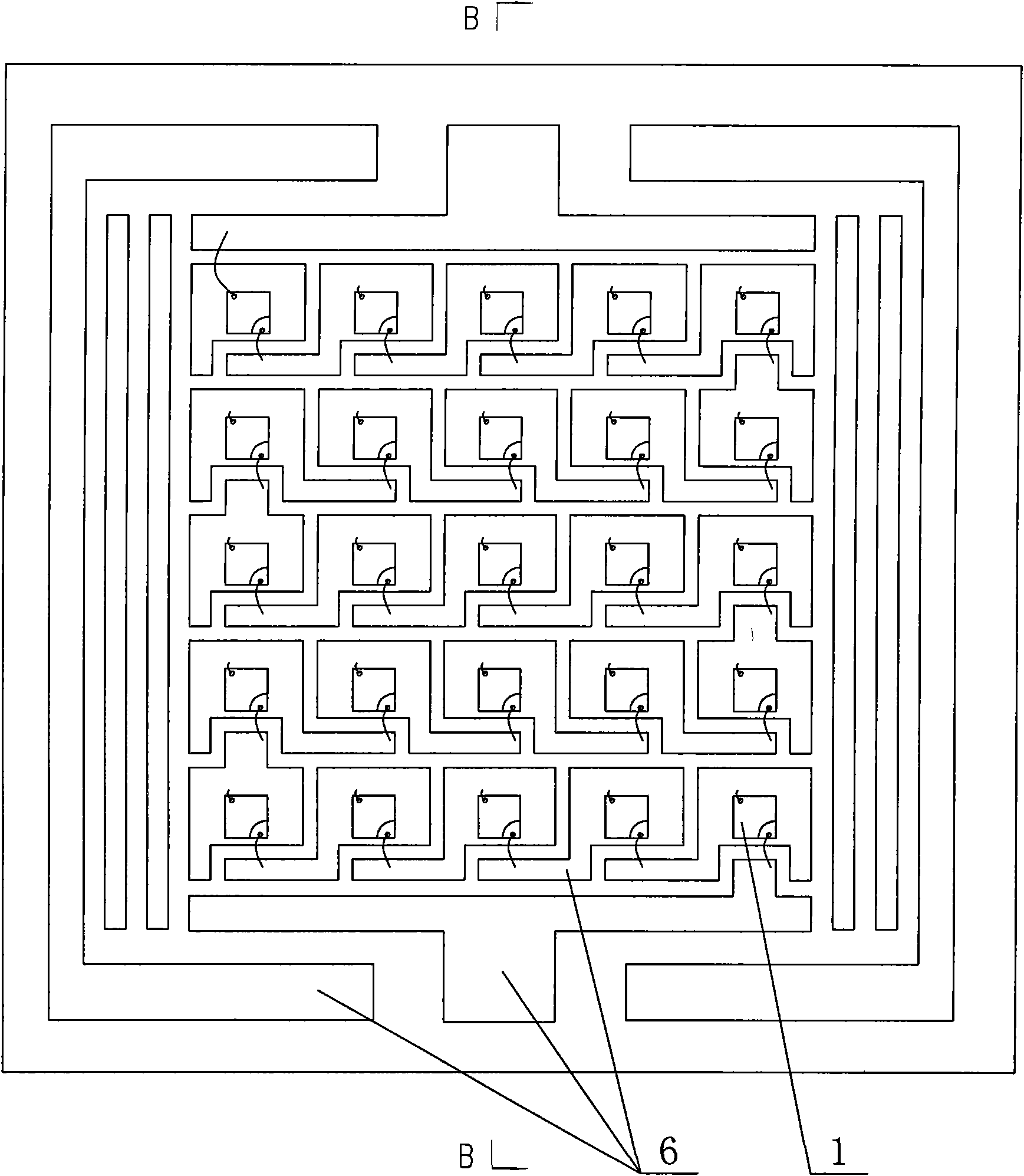
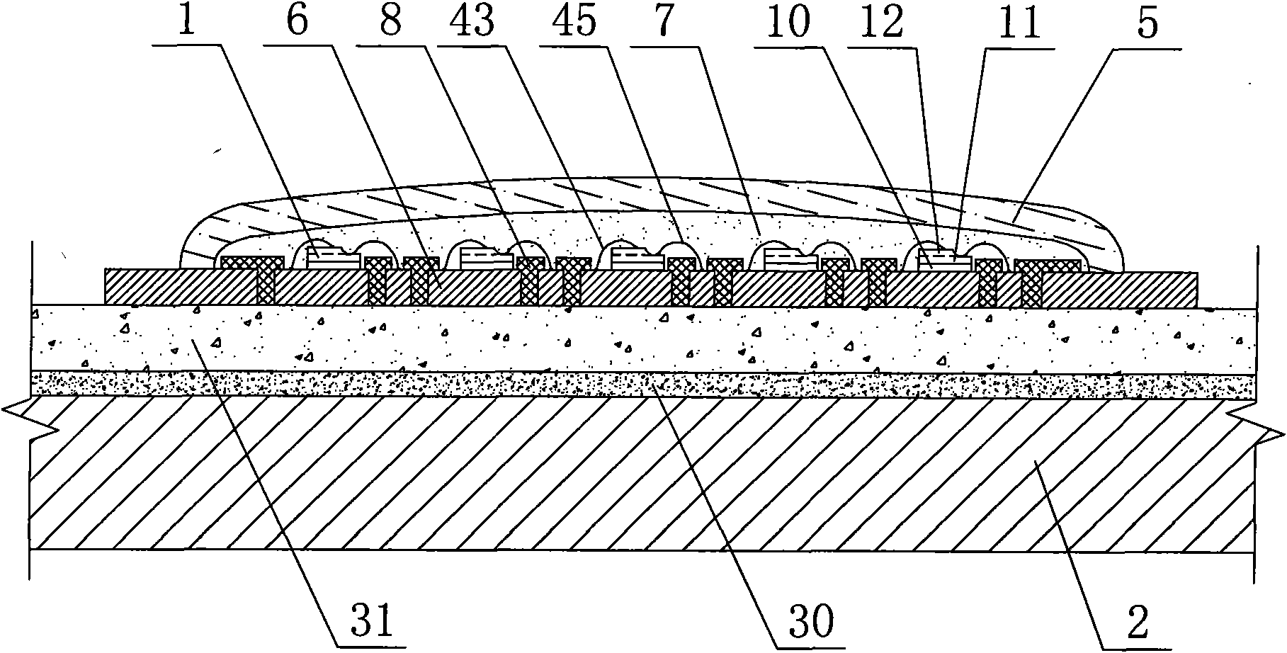
[0032] Such as Figure 1 ~ Figure 3 As shown, the high-efficiency heat dissipation LED lighting source of this embodiment is a light source applied to industrial and mining lamps with 220V alternating current, including an LED bare chip 1 and a metal substrate 2, the LED bare chip 1 is a two-electrode chip, and the LED bare chip 1 includes a substrate 10, an N-type epitaxial layer 11, and a P-type epitaxial layer 12, and the substrate 10 is aluminum oxide (sapphire, Al 2 o 3 ) substrate, of course, the substrate 10 can also be a substrate of other materials such as gallium arsenide (GaAs) or silicon carbide (SiC), and the metal substrate 2 is an aluminum substrate with a thickness of 2 mm. Of course, copper can also be used. Substrate, the thickness of the metal substrate 2 can be 1-3mm, the upper surface of the metal substrate 2 is deposited with a thermally conductive insulating layer, and a metal layer 6 is deposited on the thermally conductive insulating layer, and the up...


PUM


Abstract

The invention discloses a high-efficiency radiating LED illumination light source with low cost, good radiating effect, high production efficiency and high manufacture precision and a manufacture method. The high-efficiency radiating LED illumination light source comprises LED bare chips (1) and a metal substrate (2), wherein a heat conduction insulating layer is deposited on the metal substrate (2); metal layers (6) are deposited on the heat conduction insulating layer; the metal layers (6)are covered by a welding prevention layer (8); the heat conduction insulating layer is combined by a silicon dioxide layer (30) or a silicon nitride (31) or the combination of the silicon dioxide layer (30) and the silicon nitride (31); a preset circuit connection and a preset figure are formed on each metal layer (6) according to the serial connection and parallel connection relation of the LED bare chip (1); the LED bare chips (1) are divided into a plurality of groups and are mounted on each metal layer (6) normally or inversely; and the LED bare chips (1) in each group and the LED bare chips in the plurality of groups are connected through the metal layers (6) to form circuits. The manufacture method comprises the steps of pretreatment of the metal substrate, formation of the heat conduction insulating layer, the metal layers and the welding prevention layer as well as the encapsulation of the LED bare chips.

Description

technical field [0001] The invention relates to a high-efficiency heat dissipation LED lighting source; in addition, the invention also relates to a manufacturing method of the high-efficiency heat dissipation LED lighting source. Background technique [0002] Integrating multiple LED bare chips on a circuit board is called an integrated chip. Whether it is a single-electrode LED bare chip, a double-electrode LED bare chip or a flip-chip LED bare chip, it can be applied to an LED integrated chip. Aluminum substrates are often used in LED integrated chips. The existing lighting LED aluminum substrates use metal aluminum or aluminum alloy as a substrate, coated with an organic or inorganic thermally conductive insulating layer, and then covered with copper foil on the thermally conductive insulating layer. It is widely used in the field of LED because of its heat-conducting insulation layer can withstand high voltage (>1500V / min) and the substrate has better heat dissipati...

Claims


Application Information

Patent Timeline
Patent Type & Authority Applications(China)
IPC IPC(8): F21S2/00F21V29/00F21V23/00H01L23/36H01L33/00F21Y101/02F21K9/20
Inventor 吴俊纬
Owner NANKER GUANGZHOU SEMICON MFG
Learn More