SILICON BASED SOLID STATE LIGHTING and manufacturing method thereof

A light-emitting device and device technology, applied in semiconductor/solid-state device manufacturing, semiconductor devices, electrical components, etc., can solve the problems of providing a substrate, not using a single crystal form, and damaging the light-emitting performance of the LED structure 100, so as to prevent layer fracture , increase luminous efficiency, and improve manufacturing throughput

Inactive Publication Date: 2009-12-30
矽光光电科技有限公司
View PDF9 Cites 18 Cited by
  • Summary
  • Abstract
  • Description
  • Claims
  • Application Information

AI Technical Summary

Problems solved by technology

Another disadvantage of the conventional LED structure 100 described above is that suitable substrates such as sapphire or silicon carbide are generally not available in single crystal form.
As a result, the light emitting performance of the LED structure 100 is impaired

Method used


Image

  • SILICON BASED SOLID STATE LIGHTING and manufacturing method thereof
  • SILICON BASED SOLID STATE LIGHTING and manufacturing method thereof
  • SILICON BASED SOLID STATE LIGHTING and manufacturing method thereof

Examples


Embodiment Construction

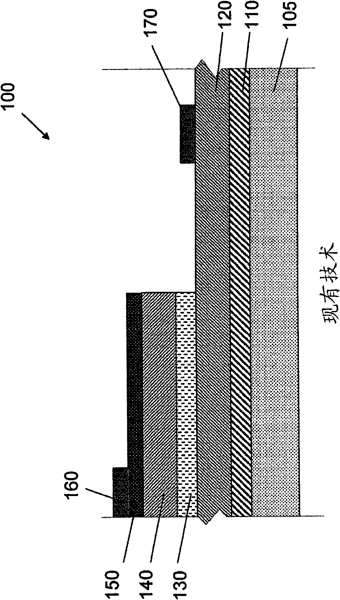
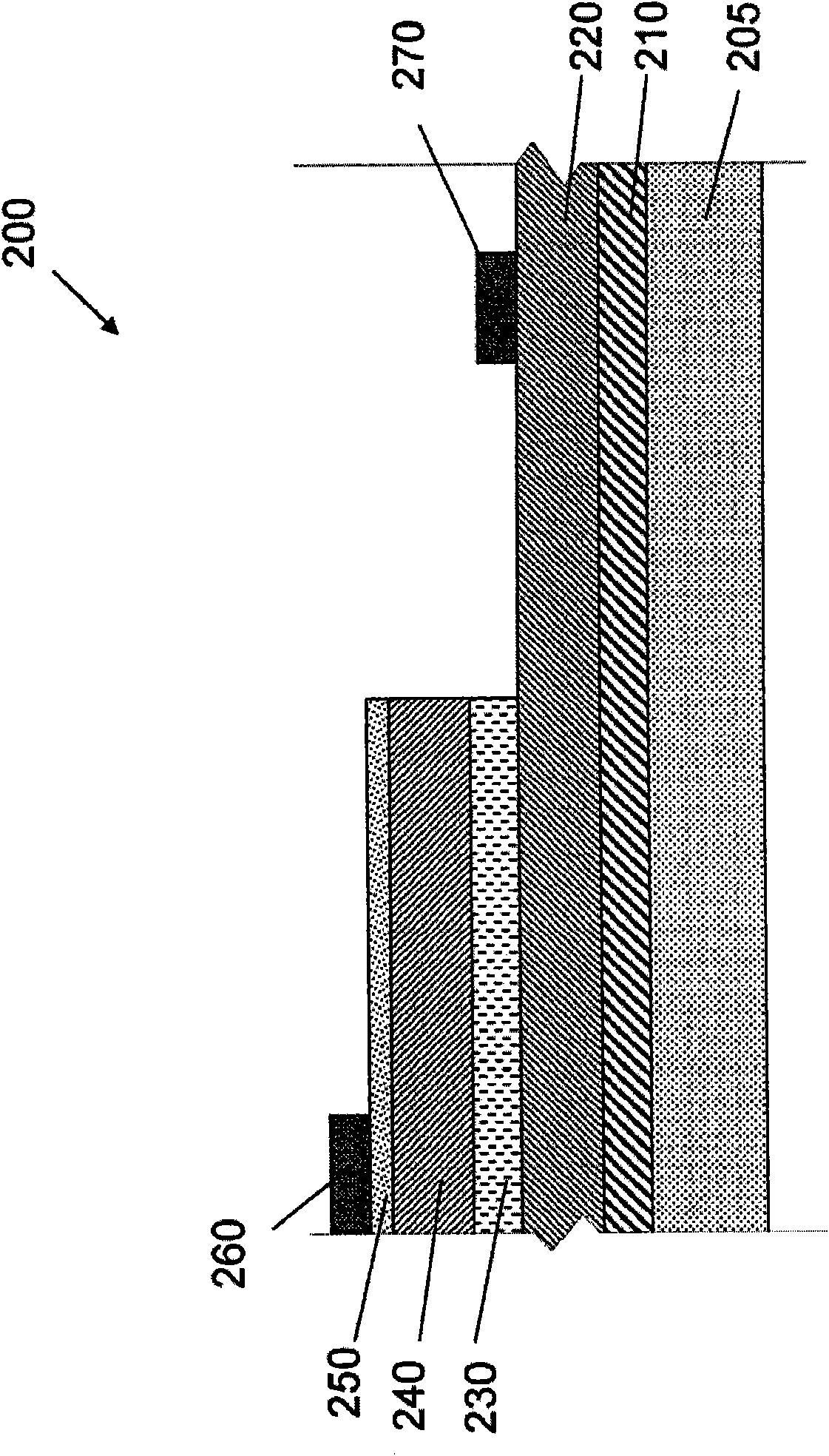
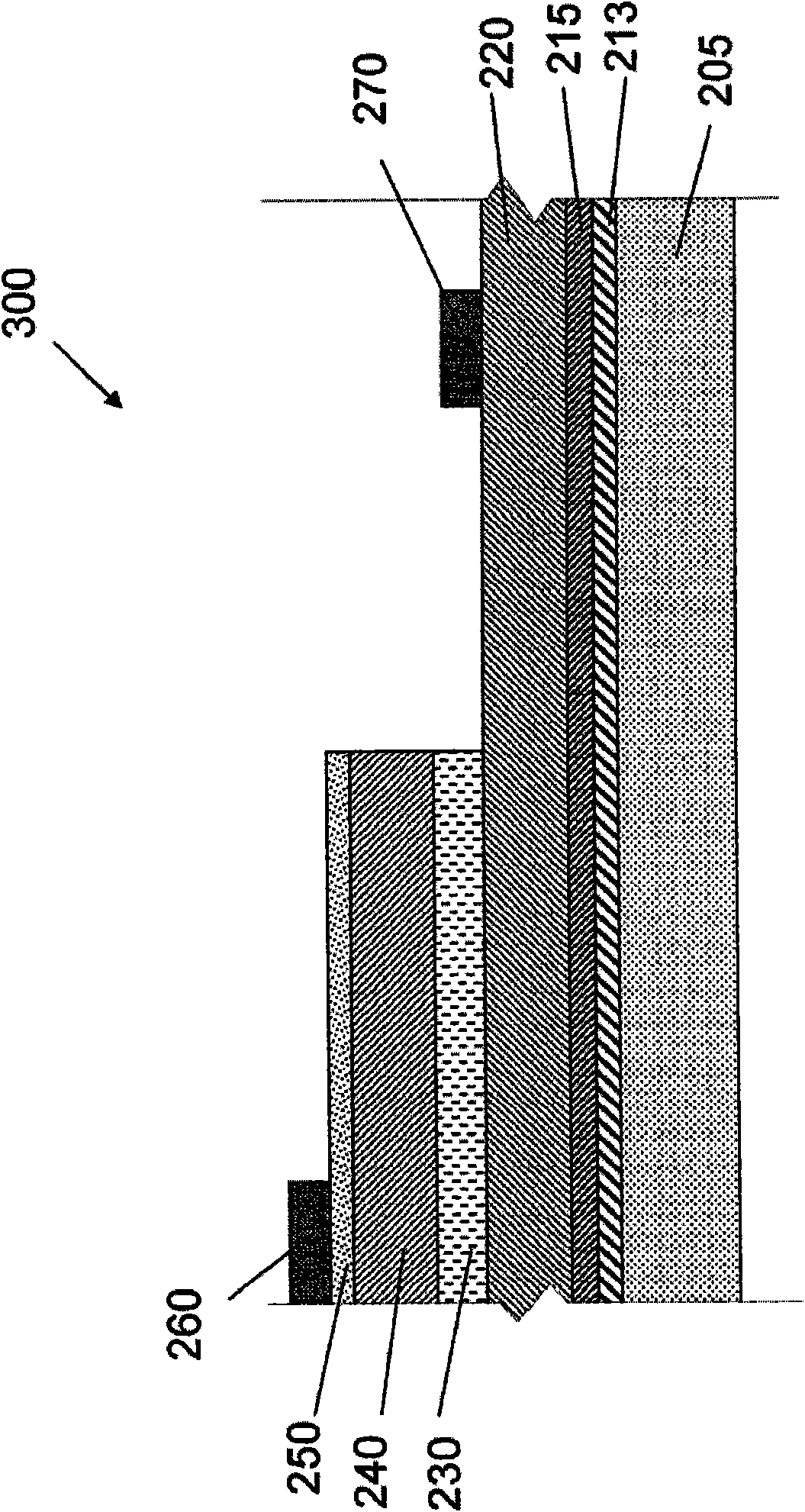
[0032] refer to figure 2 , the LED structure 200 includes a substrate 205 that may have an upper surface along a (111) or (100) crystallographic orientation. The substrate 205 may be formed of silicon, silicon oxide, or glass. For a silicon substrate, substrate 205 may include a (100) or (111) upper surface. Substrate 205 may also include a complementary metal oxide semiconductor (CMOS) material containing circuitry for driving and controlling LED structure 200 . A buffer layer (transition layer) 210 is formed on the substrate 205 . Preferably, the buffer layer 210 may include one or more optical reflective layers. The optical reflective layer may be a thin film formed of Al, Ag, Au or their oxides, or may be other multilayer metal reflective films. As another example, only one or more optical reflective layers may be formed on the substrate 205 without forming the buffer layer 210 . In addition, optionally, after one or more optical reflection layers are formed on the s...


PUM

PropertyMeasurementUnit
thicknessaaaaaaaaaa
thicknessaaaaaaaaaa

Abstract

The present invention relates to a silicon based solid state lighting. The semiconductor device includes a substrate comprising a first surface having a first orientation and a second surface having a second orientation and a plurality of III-V nitride layers on the substrate, wherein the plurality of III-V nitride layers are configured to emit light when an electric current is produced in one or more of the plurality of III-V nitride layers.

Description

technical field [0001] This patent application relates to a solid state lighting device. Background technique [0002] Solid-state light sources such as light-emitting diodes (LEDs) and solid-state lasers offer significant advantages over other forms of lighting such as incandescent or fluorescent lighting. For example, when LEDs or solid-state lasers are arranged as an array of red, green and blue elements, they can be used as a white light source or as a multicolor display. In such configurations, solid-state light sources are typically more efficient and generate less heat than traditional incandescent or fluorescent lights. Although solid-state lighting offers certain advantages, conventional semiconductor structures and devices for solid-state lighting are relatively expensive. One of the costs associated with conventional solid state lighting devices relates to the relatively low manufacturing throughput of conventional solid state lighting devices. [0003] refer t...

Claims


Application Information

Patent Timeline
Patent Type & Authority Applications(China)
IPC IPC(8): H01L33/00H01L33/12H01L33/16
CPCH01L21/02439H01L21/0243H01L21/02502H01L21/02433H01L33/12H01L33/16H01L33/007H01L21/02381H01L21/0237H01L21/0254
Inventor 潘晓和
Owner 矽光光电科技有限公司
Why Eureka
Try Eureka