Preparation method of organic electroluminescent devices
An electroluminescent device, an organic technology, applied in the direction of electric solid-state devices, semiconductor/solid-state device manufacturing, electrical components, etc., can solve the problems of low yield and achieve the effects of reduced production costs, uniform luminescence, and fewer processes
- Summary
- Abstract
- Description
- Claims
- Application Information
AI Technical Summary
Problems solved by technology
Method used
Image
Examples
preparation example Construction
[0014] The preparation method of the organic electroluminescence device of the present invention comprises:
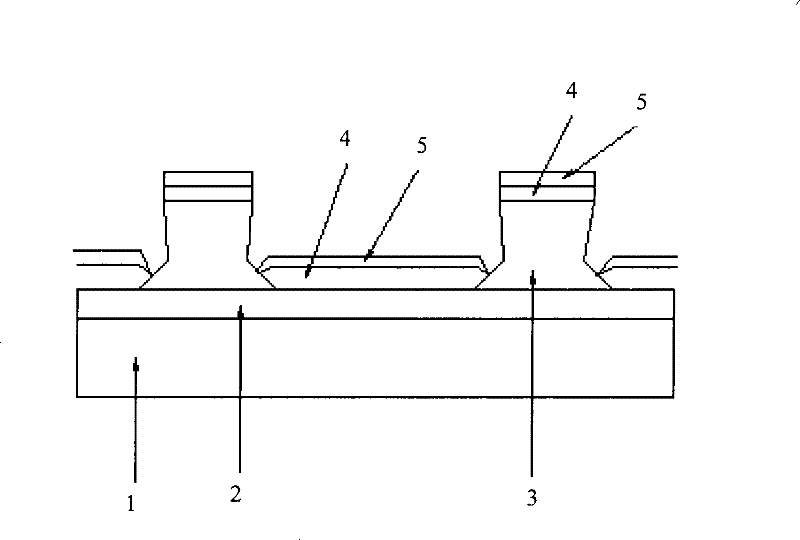
[0015] A group of parallel electrode strips are formed on the substrate, and the anodes are formed by these parallel electrode strips; a photosensitive organic polymer layer is covered on the electrode strips and the substrate between the electrode strips, and the resulting photosensitive organic polymer layer Perform masking, exposure and development to obtain a set of parallel isolation columns;
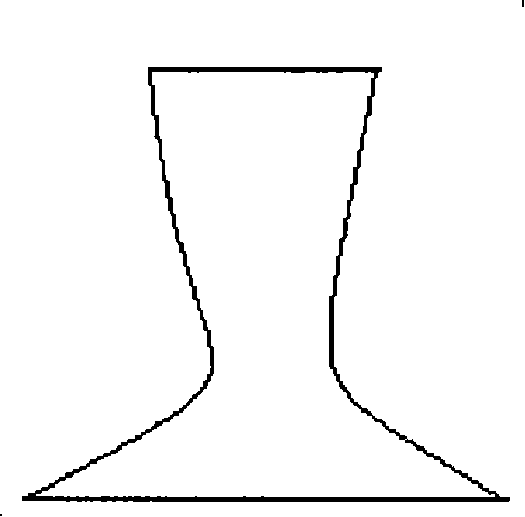
[0016] The conditions of the mask, exposure and development make the width of the upper surface of the formed isolation column 20 μm-100 μm, the shortest distance between the upper surfaces of two adjacent isolation columns is 200 μm-800 μm, the upper surface of the isolation column The width of the surface is smaller than the width of the bottom surface, the middle minimum width of the spacer column is less than or equal to the width of the upper surface, the length direct...
Embodiment 1
[0036] This example illustrates the organic electroluminescent device of the present invention and its preparation method.
[0037] (1) Preparation of anode
[0038] Indium tin oxide (ITO) film with a thickness of 150nm was formed by sputtering on a glass substrate (Leybold Hi-Tech, ITO_B0.7_STN25_R), and then a group of parallel electrode strips were formed by photolithography. The line width of the electrode strips was 500μm. The pitch is 40 μm. Then, wash and dry.
[0039] (2) Preparation of isolation column
[0040] Spin coat one layer of photosensitive polyimide (Beijing Bomi Technology Co., Ltd.) slurry on the anode that step (1) forms, then carry out pre-baking process, the temperature of described pre-baking is 110 ℃, the time of pre-baking is 15 min; forming a photosensitive polyimide layer with a thickness of 10 μm on the anode.
[0041] Then the stainless steel mask plate (Shenzhen Shuoke screen plate Co., Ltd.) is aligned with the photosensitive polyimide layer...
Embodiment 2
[0053] Prepare an organic electroluminescent device according to the method of Example 1, the difference is that step (2) is implemented as follows:
[0054] Spin coat one layer of photosensitive polyimide (Beijing Bomi Technology Co., Ltd.) slurry on the anode that step (1) forms, then carry out pre-baking process, the temperature of described pre-baking is 110 ℃, the time of pre-baking is 15 min; forming a photosensitive polyimide layer with a thickness of 3 μm on the anode.
[0055] Then the stainless steel mask plate (Shenzhen Shuoke screen plate Co., Ltd.) is aligned with the photosensitive polyimide layer of the glass substrate. The pattern of the mask plate makes the width of the upper surface of the spacer column 90 μm, adjacent to each other. The shortest distance between the upper surfaces of two spacers is 200 μm. Expose the glass substrate by UV light (245nm) with an exposure dose of 20mJ / cm 2 , the exposure time is 8s;
[0056] The exposed glass substrate is po...
PUM
 Abstract
Description
Claims
Application Information


