Pressure sensor

A pressure sensor and piezoresistive element technology, applied in the measurement of fluid pressure, instruments, and fluid pressure measurement through electromagnetic elements, can solve problems such as dependence and measurement error, and achieve the effect of improved sensitivity and high measurement accuracy

Inactive Publication Date: 2010-01-13
EHNDRESS KHAUZER GMBKH KO KG
View PDF1 Cites 16 Cited by
  • Summary
  • Abstract
  • Description
  • Claims
  • Application Information

AI Technical Summary

Problems solved by technology

[0011] However, this method has the disadvantage that a temperature-dependent stress state occurs on the front side of the membrane exposed to the pressure to be measured during the measurement operation, due to the different thermal expansion coefficients of silicon and the buried oxide layer and the caused by the different geometries of the two membrane sides
These stress states are temperature dependent and lead to measurement errors

Method used


Image

  • Pressure sensor
  • Pressure sensor
  • Pressure sensor

Examples


Embodiment Construction

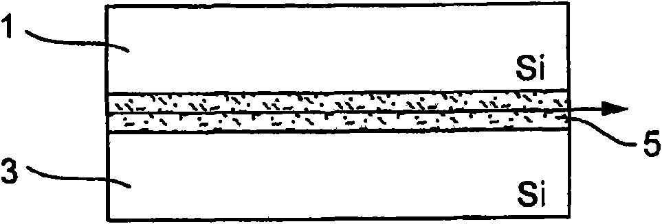
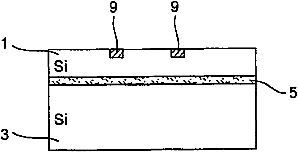
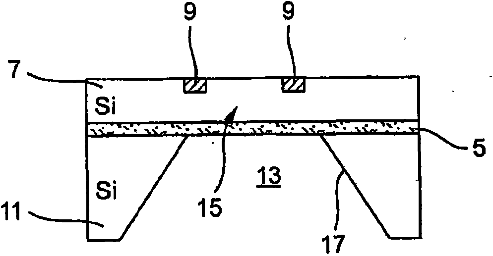
[0049] The pressure sensor of the present invention is a semiconductor sensor on a silicon substrate, which is produced by using silicon-on-insulator (SOI) technology. Here, the conventional BESOI (Bonded and etchback silicon on insulator: silicon wafer bonding and backside etching) wafer is used as the starting material. BESOI wafers are produced, for example, from two silicon oxide wafers which are oriented opposite and bonded under pressure and high temperature. In this way, obtaining a figure 1 A three-layer wafer is shown having first and second silicon layers 1,3. An oxide layer 5 is located between the first and second silicon layers 1,3. The buried oxide layer 5 is called BOX (Buried oxide layer), and its thickness is several nm to several μm.

[0050] This compound is thinned and polished from one side. The thinned and polished side forms the active layer 7 . The active layer can be several μm thick and is called, for example, device wafer or silicon overlayer (S...


PUM

PropertyMeasurementUnit
thicknessaaaaaaaaaa

Abstract

The invention relates to a piezo-resistive pressure sensor in BESOI technology, which is particularly suited for measuring low pressures, has low linearity distortion, is made of a BESOI wafer having a first and a second silicon layer (1, 3) and an oxide layer (5) disposed between the same, has an active layer (7) that is formed by a first silicon layer (1) of the BESOI wafer, piezo-resistive elements (9) being doped in said active layer, and has a membrane carrier (11) formed by the second silicon layer (3) of the BESOI wafer, the carrier surrounding a recess (13) in the second silicon layer (3) on the outside, the recess exposing a region of the active layer (7) forming a membrane (15) and of the associated oxide layer (5), wherein in an outer edge of the region (21) of the oxide layer (5) exposed by the recess (13) a groove (19) surrounding the region (21) is provided.

Description

technical field [0001] The invention relates to a pressure sensor. Background technique [0002] Pressure sensors are used to detect pressure and are used, for example, in pressure measuring instruments used in industrial measuring technology. [0003] In pressure measurement technology, so-called semiconductor sensors, such as silicon chips doped with piezoresistive resistance elements, are commonly used as pressure sensors. Semiconductor sensors of this type comprise a measuring membrane arranged on a carrier, one side of which is exposed to the pressure to be measured during measuring operation. Typically, pressure sensor chips are very sensitive and are thus not directly exposed to the medium in which the pressure is to be recorded. Instead, a pressure transmission device filled with liquid is inserted. The pressure acting on the measuring membrane causes a pressure-dependent deflection of the measuring membrane, which is detected by the doped resistive element and co...

Claims


Application Information

Patent Timeline
Patent Type & Authority Applications(China)
IPC IPC(8): G01L9/06
CPCG01L9/0055G01L9/0042
Inventor 伊戈尔·格特曼迪特尔·施托尔塞英·图安·塔姆
Owner EHNDRESS KHAUZER GMBKH KO KG
Why Eureka
Try Eureka