Semiconductor device and method of manufacturing same
A manufacturing method and semiconductor technology, which can be used in the manufacture of semiconductor/solid-state devices, semiconductor devices, and electric solid-state devices, etc., can solve problems such as the occurrence of oxygen defects, the reverse charge amount of the ferroelectric film, or the deterioration of the leakage current value, and achieve improved characteristics. Effect
- Summary
- Abstract
- Description
- Claims
- Application Information
AI Technical Summary
Problems solved by technology
Method used
Image

Examples
no. 1 approach
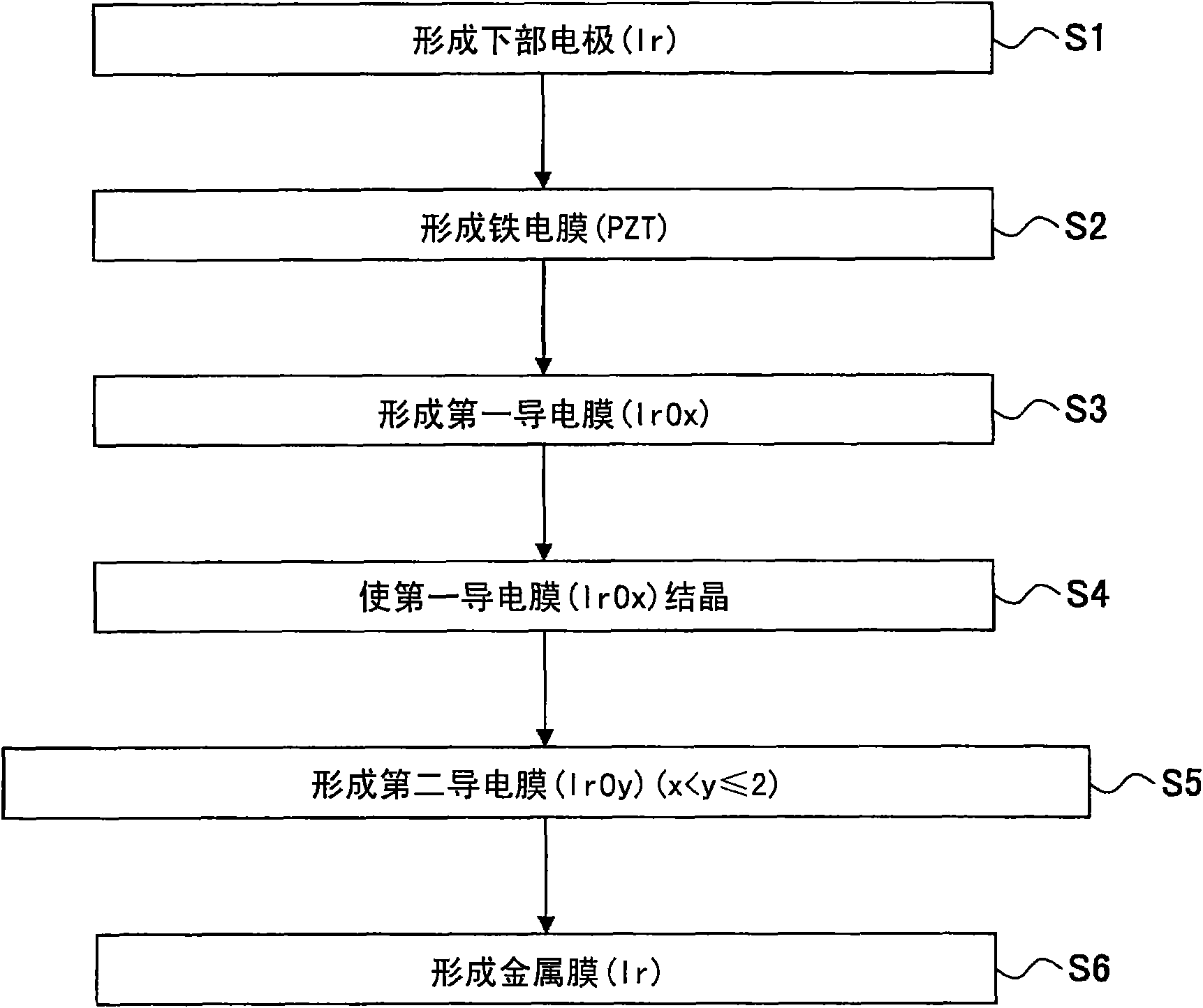
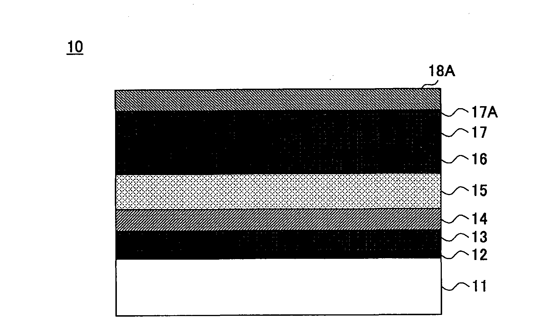
[0121] Figure 3A It is a figure which shows the structure of the ferroelectric capacitor 10 of 1st Embodiment of this invention.
[0122] refer to Figure 3A , the ferroelectric capacitor 10 is composed of an orientation control film 12, a conductive oxygen barrier film 13, a lower electrode 14, a ferroelectric film 15, a conductive oxide film 16, a conductive oxide film 17, a stoichiometric composition region 17A, and a metal film 18, and The conductive oxide film 16 and the conductive oxide film 17 including the stoichiometric composition region 17A are formed together with the metal film 18 Figure 3A The upper electrode of the ferroelectric capacitor 10 in the above, wherein the orientation control film 12 is formed on a silicon oxide film 11 for covering a silicon substrate (not shown), and is formed on the silicon oxide film 11 with ( 111) Oriented TiN film or Ti film with (002) orientation is used to control the crystallographic orientation of the ferroelectric capac...
no. 2 approach
[0174] Below, refer to Figure 12 A to 12V will describe the manufacturing process of the ferroelectric memory according to the second embodiment of the present invention.
[0175] refer to Figure 12 A. An n-type well is formed in the silicon substrate 61 as an element region 61A, and a first MOS transistor having a polysilicon gate electrode 63A and a polysilicon gate electrode 63B are formed on the element region 61A via gate insulating films 62A and 62B, respectively. of the second MOS transistor.
[0176] Further, in the silicon substrate 61, p is formed on both sidewall surfaces corresponding to the gate electrode 63A. - type LDD regions 61a and 61b, and p is formed on both sidewall surfaces corresponding to the gate electrode 13B. - type LDD regions 61c and 61d. Here, since the first and second MOS transistors are formed together in the element region 61A, they share the same p - Type diffusion regions serve as the LDD region 61b and the LDD region 61c.
[0177] A...
no. 3 approach
[0208] Figure 13 The structure of the ferroelectric memory of the third embodiment of the present invention is shown. In the drawings, the same reference numerals are assigned to the parts described above, and the description thereof is omitted.
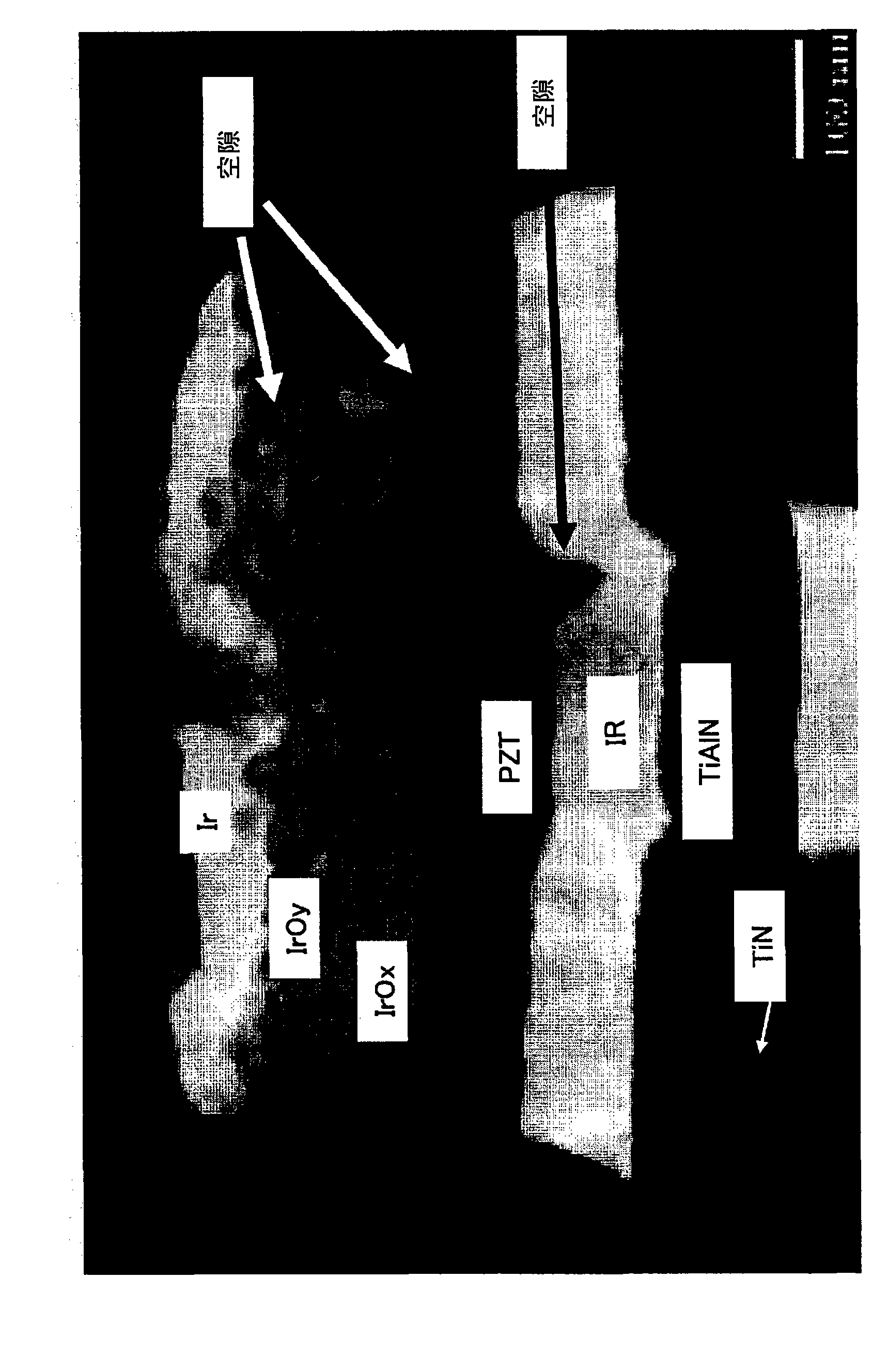
[0209] previously explained Figure 12 In the embodiment of A to 12V, in Figure 12 In step B, the through-hole inserts 69A and 69C are formed by filling the through-holes 68A and 68C with a tungsten film, and then removing the excess tungsten film on the interlayer insulating film 68 by CMP. It is difficult to completely flatten the surfaces of the through-hole inserts 69A and 69B by such a CMP method, and concave portions having a depth of 20 to 50 nm are usually formed in the upper portions of the through-hole inserts 69A and 69C.
[0210] Since such a concave portion has a great influence on the crystal orientation of the ferroelectric capacitor formed thereon, in the present embodiment, the above-mentioned Figure 12 After ...
PUM
| Property | Measurement | Unit |
|---|---|---|
| thickness | aaaaa | aaaaa |
| thickness | aaaaa | aaaaa |
| thickness | aaaaa | aaaaa |
Abstract
Description
Claims
Application Information
 - R&D
- Intellectual Property
- Life Sciences
- Materials
- Tech Scout
- Unparalleled Data Quality
- Higher Quality Content
- 60% Fewer Hallucinations
Browse by: Latest US Patents, China's latest patents, Technical Efficacy Thesaurus, Application Domain, Technology Topic, Popular Technical Reports.
© 2025 PatSnap. All rights reserved.Legal|Privacy policy|Modern Slavery Act Transparency Statement|Sitemap|About US| Contact US: help@patsnap.com