Reacting chamber and plasma processing system with same

A reaction chamber and chamber technology, applied in the field of microelectronics, can solve the problems affecting the processing/processing results of workpieces, process yield rate, pumping speed, affecting workpiece processing/processing results, and affecting process yields, etc., to avoid Airflow reflection and turbulence, reduced pumping time, effect of reduced pumping time

Inactive Publication Date: 2010-02-03
BEIJING NAURA MICROELECTRONICS EQUIP CO LTD
View PDF0 Cites 5 Cited by
  • Summary
  • Abstract
  • Description
  • Claims
  • Application Information

AI Technical Summary

Problems solved by technology

Due to the limited size of the outlet, the reflection of the airflow occurs near the outlet (as shown by the dotted circle at the interface in the figure), and causes the airflow to form turbulent flow inside the chamber, so that the particles deposited inside the chamber and/or The fine dust is carried and rolled up by the reflected air flow, and pollutes the processed workpiece in the chamber 3, which affects the processing/processing results of the workpiece and affects the yield of the process
At the same time, the air flow with the above-mentioned flow direction will form a flow bottleneck

Method used


Image

  • Reacting chamber and plasma processing system with same
  • Reacting chamber and plasma processing system with same
  • Reacting chamber and plasma processing system with same

Examples


Embodiment Construction

[0029] In order to enable those skilled in the art to better understand the technical solutions of the present invention, the reaction chamber and the plasma processing system provided with the reaction chamber provided by the present invention will be described in detail below with reference to the accompanying drawings.

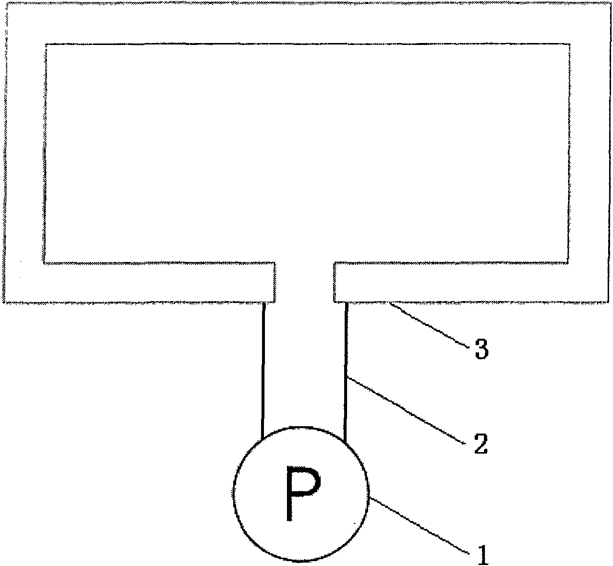
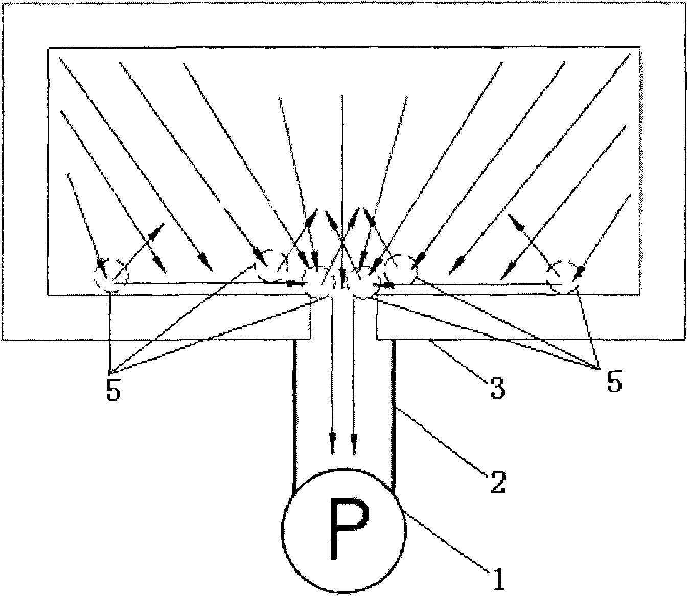
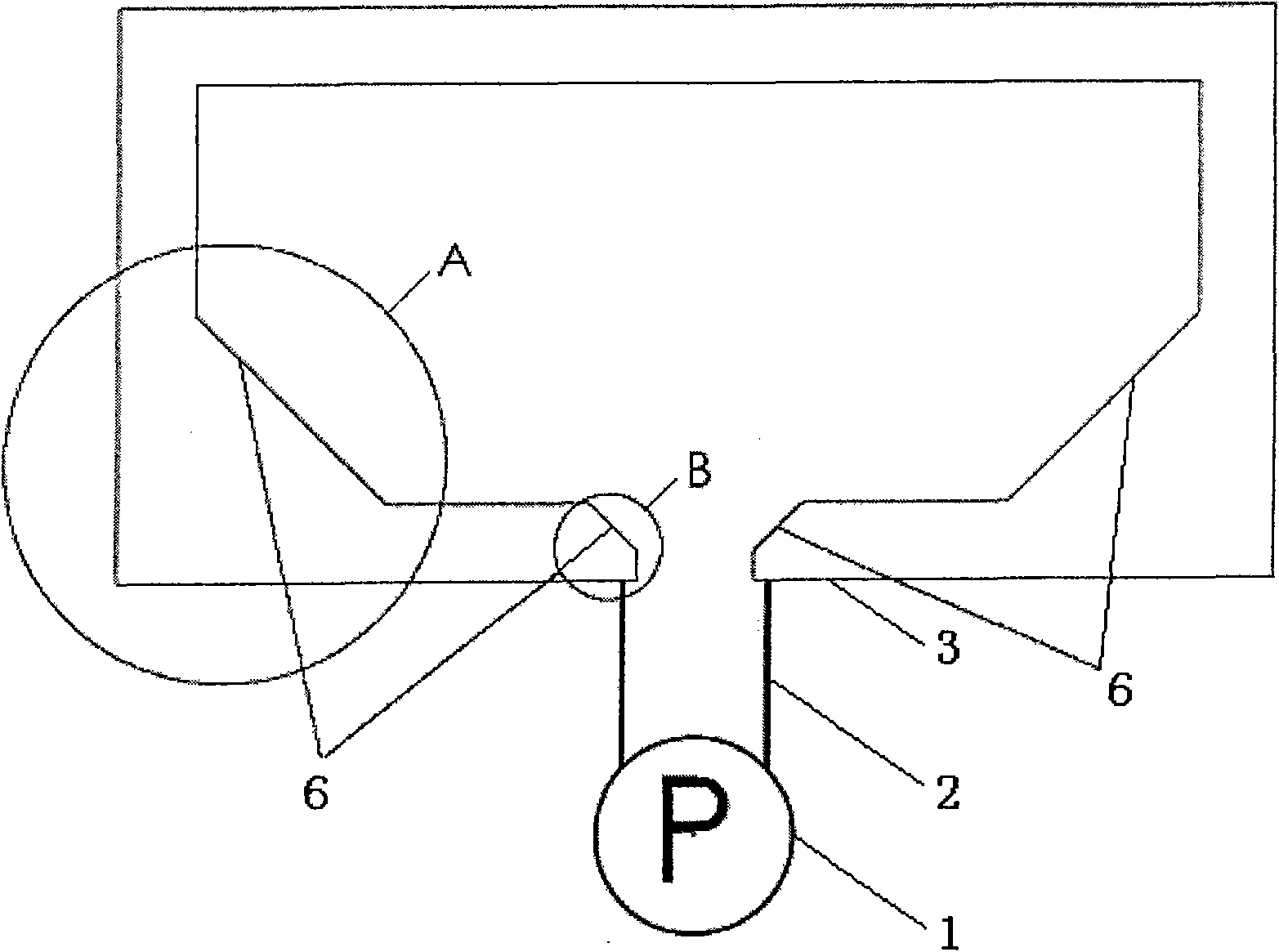
[0030] see image 3 , which shows the reaction chamber provided by the first embodiment of the present invention. Let’s take the left half of the chamber 3 as an example for illustration. The positions of the inner walls A and B of the chamber are designed as inclined plane structures 6. The inclined plane structures 6 follow the flow direction of the air flow and are located at the corners of the chamber. The bevel structure 6 is used at the inward corner position shown by the symbol B, and the bevel structure 6 is also used at the outward corner position shown by the symbol B.

[0031] In this embodiment, the slope angle is approximately 45 degrees, that...


PUM


Abstract

The invention discloses a reacting chamber. The chamber is provided with a vacuum pump port connected with a vacuum pump, and is provided with a guide part corresponding to a turning position in the chamber, wherein the shape and the arrangement direction of the guide part conform to the air flow direction in the chamber for reducing and even preventing air flow in the chamber from generating reflection and onflow phenomenon. Furthermore, the invention also provides a plasma processing system with the reacting chamber. The reacting chamber and the plasma processing system can reduce and even avoid particulate pollution in the chamber so as to improve the manufacturing/processing quality of a workpiece, technical yield and air exhaust velocity.

Description

technical field [0001] The invention relates to the technical field of microelectronics, in particular, to a reaction chamber and a plasma processing system with the reaction chamber. Background technique [0002] With the rapid development of electronic technology, people have higher and higher requirements for the integration of integrated circuits, which requires companies that produce integrated circuits to continuously improve the processing / processing capabilities of semiconductor devices. Currently, plasma processing techniques such as plasma deposition techniques, plasma etching techniques, and the like are widely used in the processing / processing of semiconductor devices. These plasma processing technologies usually need to be realized by means of corresponding plasma processing systems. [0003] Generally, a reaction chamber for providing a vacuum environment is provided in the above-mentioned plasma processing system. In practical applications, in order to obtai...

Claims


Application Information

Patent Timeline
IPC IPC(8): H01L21/00H01L21/02B01J3/03H01J37/32H05H1/00C23C16/00C23F4/00
Inventor 张之山
Owner BEIJING NAURA MICROELECTRONICS EQUIP CO LTD
Why Eureka
Try Eureka