Method for repairing and etching polysilicon

A technology of polysilicon and plasma, applied in electrical components, semiconductor/solid-state device manufacturing, circuits, etc., can solve the problems of lower yield, unevenness, and substrate damage of source and drain, so as to improve yield and ensure reliability , the effect of good etching uniformity

Inactive Publication Date: 2010-03-10
SEMICON MFG INT (SHANGHAI) CORP
View PDF0 Cites 16 Cited by
  • Summary
  • Abstract
  • Description
  • Claims
  • Application Information

AI Technical Summary

Problems solved by technology

[0004] However, in the restoration etching process of step S16, the method of plasma physical bombardment is currently mainly used for etching, and the etching reaction chamber is mainly filled with Ar 2 gas and a small amount of O 2 、CF 4 , Ar plasma is formed in the chamber, and Ar ions bombard the surface under the action of electric field acceleration. Since the surface after silicon oxide is etched in step S15 is mainly a silicon substrate, Ar is an inert atom, so it will not chemically etch with surface substances. Etching, mainly through physical bombardment, etch the residual oxide dielectric and polymer components, but we also found that this repair etching method will etch away the silicon that will be used to form the source and drain In the substrate region, the substrate silicon in the source and drain regions will be etched away by 1-15nm, so that the substrate used to form the source and drain is damaged, the pn junction between the source and the substrate, and the drain and the substrate The pn juncti

Method used


Image

  • Method for repairing and etching polysilicon
  • Method for repairing and etching polysilicon
  • Method for repairing and etching polysilicon

Examples


Example Embodiment

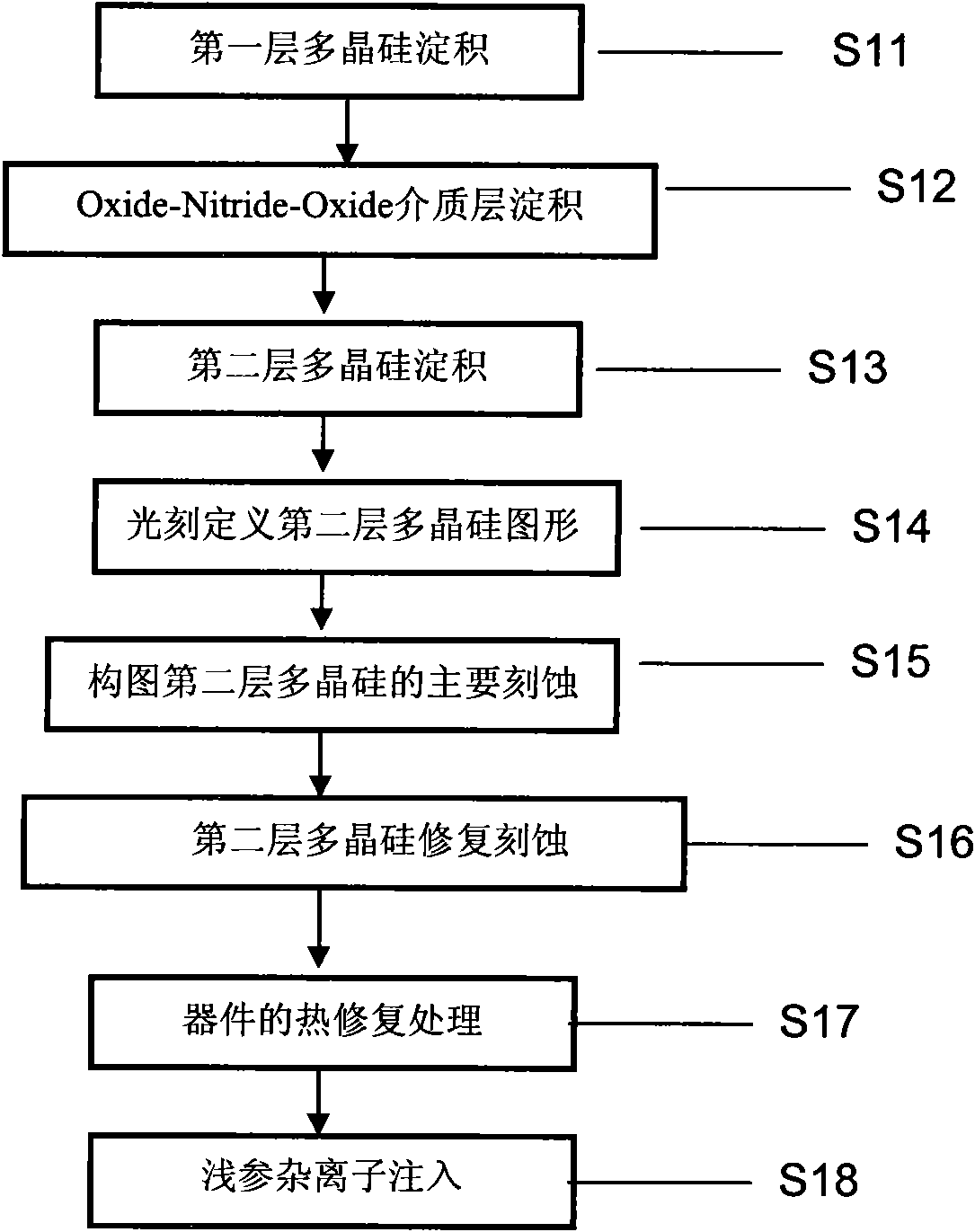
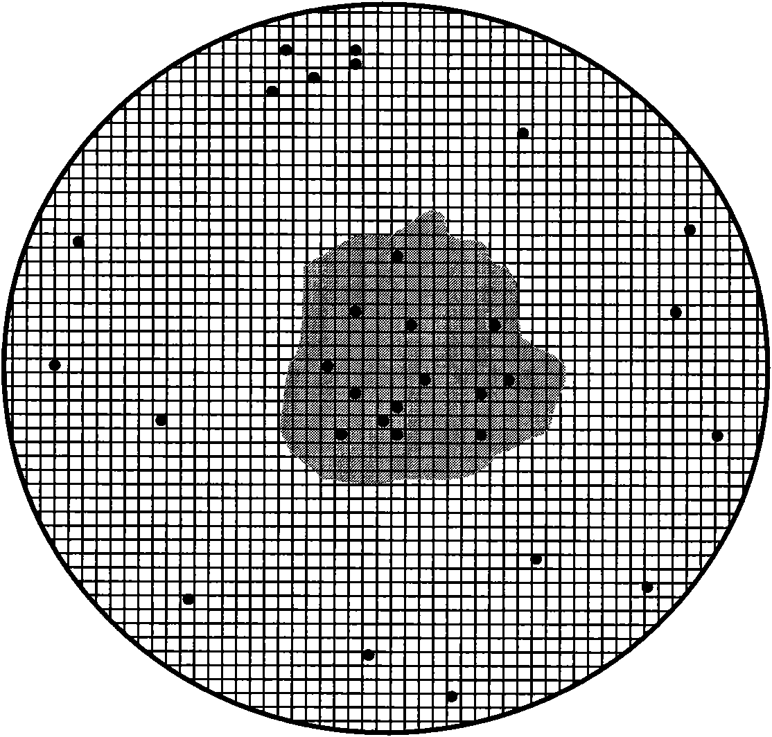
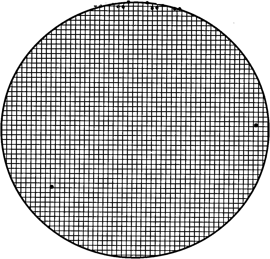
[0011] This embodiment describes the repair etching method of the control gate polysilicon of EEPROM under the 0.35um process technology generation, according to figure 1 The manufacturing process of the gate of the shown EEPROM, in the manufacturing process of the EEPROM, the main etching step of S16 is mainly to pattern and etch the second layer of polysilicon and the Oxide-Nitride-Oxide dielectric layer under the second layer of polysilicon, wherein The substrate silicon is used as the etching stop layer, and the second layer of polysilicon is repaired and etched after step S16, and the second layer of polysilicon is used to form the control gate of the EEPROM.

[0012] The polysilicon etching method of this embodiment is completed in a kind of plasma dry etching equipment. During the etching process, oxygen O2 flows into the equipment chamber simultaneously. 2 and tetrafluoromethane CF 4 Two gases, O 2 with CF 4 The flow ratio scope of gas is 4: 1-6: 1, preferred O in t...


PUM


Abstract

The invention discloses a method for repairing and etching polysilicon, which belongs to the technical field of microelectronics manufacturing. The method provided by the invention is used for repairing and etching the polysilicon forming a control grid in an EEPROM and is characterized by only adopting a mixed chemical gas of O2 and CF4 for plasma etching. The etching method is a chemical etchingand has a extremely low substrate silicon etching speed, thereby avoiding damaging a pn junction between a source electrode and a substrate and a pn junction between a drain electrode and the substrate and consequently ensuring the reliability of the EEPEOM device and improving the yield of product.

Description

technical field [0001] The invention belongs to the technical field of microelectronics manufacturing, and in particular relates to a method for repairing and etching polysilicon. Background technique [0002] Electrically Erasable Programmable Read-Only Memory (EEPROM) is a non-volatile memory whose gate structure has a floating gate (Polysilicon) material and a control gate (Control Gate), floating gate and control gate There is a dielectric layer structure of silicon oxide-silicon nitride-silicon oxide (Oxide-Nitride-Oxide) between them, which is used to trap charges. [0003] In the current fab, the main manufacturing process of the gate of EEPROM is as follows: figure 1 As shown, after the channel doping of EEPROM is preliminarily completed, the first layer of gate dielectric layer is formed by patterning, and further, in step S11, the first layer of polysilicon is deposited on the first layer of gate dielectric, and the first layer of polysilicon is patterned and etch...

Claims


Application Information

Patent Timeline
IPC IPC(8): H01L21/3065C23F4/00
Inventor 王芳周朝锋张凯元田三河
Owner SEMICON MFG INT (SHANGHAI) CORP
Why Eureka
Try Eureka