Separated grid type embedded layer float grid nonvolatile storage unit and manufacturing method thereof

A non-volatile storage and floating gate technology, which is applied in semiconductor/solid-state device manufacturing, electrical components, electric solid-state devices, etc., can solve the problem of difficult shrinkage of vertical structure, unfavorable integration and miniaturization of memory cells, and short trench of MOS transistors. channel and other issues, to achieve the effect of improving charge coupling, avoiding short channel effects, and increasing effective distance

Active Publication Date: 2010-03-10
SHANGHAI HUAHONG GRACE SEMICON MFG CORP
View PDF1 Cites 10 Cited by
  • Summary
  • Abstract
  • Description
  • Claims
  • Application Information

AI Technical Summary

Problems solved by technology

[0004] First of all, since the split-gate structure in the memory cell structure is located on the semiconductor substrate, the effective channel length of the MOS transistor is also correspondingly reduced as the feature size of the memory cell shrinks, which easily causes the short channel of the MOS transistor in the cell. effect, which destroys the normal storage function of the MOS transistor in the unit, and even leads to the failure of the storage unit
[0005] Secondly, since the floating gate structure is located on the semiconductor substrate, it occupies the vertical volume of the memory unit. Although the horizontal structure of the device continues to shrink with the continuous reduction of the feature size of the semiconductor manufacturing process, the vertical structure is difficult to shrink, which is not conducive to Integration and miniaturization of memory cells
[0006] Thirdly, in order to improve the erasing and writing efficiency of the memory cell, the storage structure needs to fabricate a floating gate with a cutting-edge structure. Since the manufacturing of the cutting-edge structure requires more steps and the process is more complicated, it increases the difficulty of device manufacturing.
[0007] Finally, as the size of the floating gate shrinks, when other conditions remain unchanged, the coupling rate of the source to the charge of the floating gate will decrease, thereby affecting the programming ability of the non-volatile memory cell, resulting in a non-volatile memory cell Performance drop

Method used


Image

  • Separated grid type embedded layer float grid nonvolatile storage unit and manufacturing method thereof
  • Separated grid type embedded layer float grid nonvolatile storage unit and manufacturing method thereof
  • Separated grid type embedded layer float grid nonvolatile storage unit and manufacturing method thereof

Examples


Embodiment Construction

[0032] In order to make the object, technical solution and advantages of the present invention clearer, the present invention will be further described in detail below in conjunction with the accompanying drawings.

[0033] The invention proposes a sub-gate type buried layer floating gate type non-volatile storage unit structure. It can effectively reduce the structure size of the storage unit, avoid the short channel effect and have higher programming efficiency and smaller unit thickness.

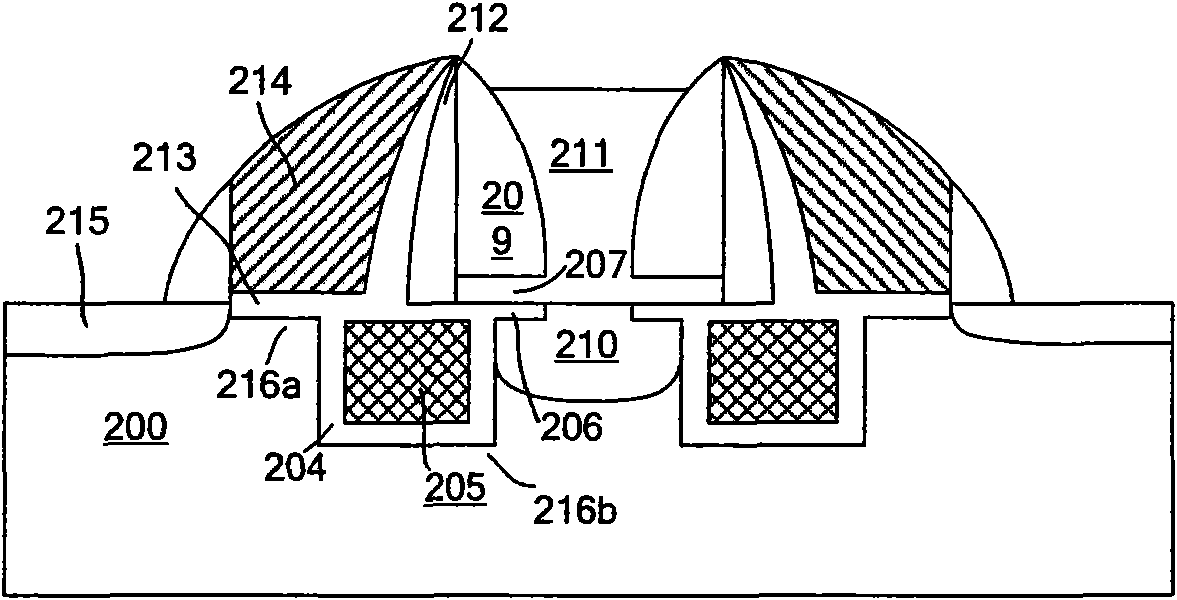
[0034] refer to figure 2Shown is a schematic diagram of a split-gate buried non-volatile memory cell structure according to a preferred embodiment of the present invention. The structure includes: a semiconductor substrate 200; channel regions 216a and 216b located between the source region 210 and drain region 215 which are separated from each other; Formed by the first conductive layer; source 211, formed by the second conductive layer and the third conductive layer, located above th...


PUM


Abstract

The invention relates to a separated grid type embedded layer float grid nonvolatile storage unit and a manufacturing method thereof. The storage unit comprises a semiconductor substrate, a source region, a drain region, a channel region, a float grid, a source electrode and a control grid. The float grid is below first insulated medium layers and fully embedded in the semiconductor substrate, a second insulated medium layer between the float grid and the semiconductor substrate is connected with the first insulated medium layers and fully enclosures the float grid. The float and the second insulated medium layer are positioned between the source region and the drain region, the second insulated medium layer is far from one side of the drain region and contacted with the source region, thechannel region comprises a first channel region which is arranged between the drain region and the second insulated medium layer along the surface of the semiconductor substrate and a second channelalong the surface of the second insulated medium layer to the source region, and first insulated medium layers are arranged between the float grid and the control grid as well as between the float grid and the source electrode, a part protruding levelly at the bottom of the source electrode is positioned above the first insulated medium layer, and a covering part is arranged in the direction vertical to the surface of the semiconductor substrate.

Description

technical field [0001] The invention relates to a semiconductor storage unit and a method for manufacturing the semiconductor storage unit, in particular to a sub-gate type buried layer floating gate type non-volatile storage unit and a manufacturing method thereof. Background technique [0002] A non-volatile memory (Non-volatile Memory, NVM) refers to a memory cell having a MOS transistor structure, and the cell structure generally includes a source region, a drain region, a channel region, a control gate and a floating gate. The floating gate structure is the main difference between the MOS transistor of the non-volatile memory unit and the ordinary MOS transistor. It plays the role of storing charge in this memory cell structure, so that the memory cell can still maintain the stored value even when the power is turned off. information, which makes this memory non-volatile. At present, the floating gate structure generally adopts a stacked or divided gate structure, and ...

Claims


Application Information

Patent Timeline
Patent Type & Authority Applications(China)
IPC IPC(8): H01L27/115H01L21/8247
Inventor 江红孔蔚然李冰寒
Owner SHANGHAI HUAHONG GRACE SEMICON MFG CORP
Why Eureka
Try Eureka