Method for manufacturing shallow junction complementary bipolar transistor

A technology of bipolar transistor and manufacturing method, which is applied in semiconductor/solid-state device manufacturing, electrical components, circuits, etc., can solve the problems of low withstand voltage of transistors, difficult to meet the high-precision and dynamic adjustment requirements of high-speed analog integrated circuits, and achieve the characteristics of The effect of increasing frequency, reducing leakage current, and increasing withstand voltage

Inactive Publication Date: 2012-05-02
NO 24 RES INST OF CETC
View PDF0 Cites 1 Cited by
  • Summary
  • Abstract
  • Description
  • Claims
  • Application Information

AI Technical Summary

Problems solved by technology

The advantage of these processes is that the characteristic frequency is high, but when applied to high-precision analog integrated circuits, the withstand voltage of its transistors is low (BV CEO <3.0V, it is difficult to meet the high-precision and dynamic adjustment requirements of higher-voltage high-speed analog integrated circuits

Method used


Image

  • Method for manufacturing shallow junction complementary bipolar transistor
  • Method for manufacturing shallow junction complementary bipolar transistor
  • Method for manufacturing shallow junction complementary bipolar transistor

Examples


Embodiment Construction

[0045] The specific embodiments of the present invention are not limited to the following description. The present invention will now be further described with reference to the drawings.

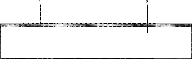
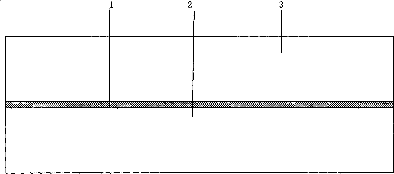
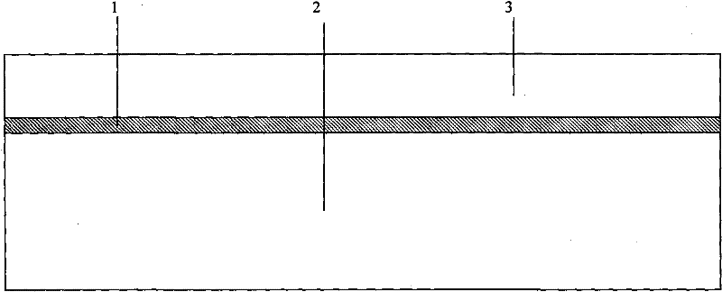
[0046] The method of the present invention first uses silicon / silicon bonding, CMP thinning and polishing technology to obtain the required SOI material sheet, and then forms the SOI material sheet by implanting a buried layer, decompressing ultra-thin epitaxy, deep trench etching, and polysilicon backfilling. The deep trench dielectric isolation plus shallow isolation wall technology, combined with the complementary bipolar process compatible with the vertical PNP of the shallow junction polysilicon emitter and the vertical NPN, is used to manufacture the shallow junction complementary bipolar transistor.

[0047] 1. The steps of forming SOI material sheet by silicon / silicon bonding, thinning and polishing method are:

[0048] 1# liquid (NH) for P-type silicon wafer 2 with crystal orientation an...


PUM


Abstract

The invention discloses a method for manufacturing a shallow junction complementary bipolar transistor. The main technological steps of the method are as follows: 1) forming an SOI material chip by the methods of silicon / silicon bonding, thinning and polishing; and 2) manufacturing the shallow junction complementary bipolar transistor by using the methods of deep-trench etching, deep trench isolation with polysilicon backfilling and a shallow isolation wall and combining with a longitudinal NPN pipe with a shallow junction polysilicon emitter and the complementary bipolar technology which is compatible with the longitudinal PNP pipe. The method improves the pressure resistance (BVCEO is greater than 5.0V) and the Early voltage of the complementary bipolar transistor and simultaneously takes into consideration of the characteristic frequency. The method greatly reduces the drain current of an isolation junction, and the drain current of the shallow junction complementary bipolar transistor is smaller than 10<minus 12>A. The method can be widely applied in the field of manufacture of high-speed complementary bipolar technologies.

Description

Technical field [0001] The invention relates to a method for manufacturing a shallow junction complementary bipolar transistor, and its direct application field is the field of high-speed complementary bipolar transistor manufacturing. Background technique [0002] The complementary bipolar process (CB) has a history of more than 30 years. In the early days, the PNP tube and the NPN tube were mainly used to form a complementary structure, and the junction isolation CB process was adopted around 1986. The main advantage of the CB process is that high frequency vertical NPN and PNP transistors with extremely small parasitic capacitance can be obtained at the same time. This complementary bipolar transistor has a very high characteristic frequency f at a certain current. T Therefore, the integrated operational amplifier can have better frequency characteristics and bandwidth characteristics under a small quiescent current. However, the complementary bipolar process is difficult to m...

Claims


Application Information

Patent Timeline
Patent Type & Authority Patents(China)
IPC IPC(8): H01L21/84
Inventor 李荣强崔伟张正元
Owner NO 24 RES INST OF CETC
Why Eureka
Try Eureka