Copper, copper/molybdenum, or copper/molybdenum alloy electrode etching solution for use in liquid crystal display system

A technology of molybdenum alloy and etching solution, which is applied in the direction of instruments, circuits, electrical components, etc., can solve the problems of etching process aging changes, explosive pipeline systems, and the stability of etching solution, etc., and achieve excellent etching profile and stable process operation , good flatness effect

Active Publication Date: 2010-03-31
SOULBRAIN CO LTD
View PDF0 Cites 65 Cited by
  • Summary
  • Abstract
  • Description
  • Claims
  • Application Information

AI Technical Summary

Problems solved by technology

In this case, it can easily control the etch rate, consistently obtain the desired taper, obtain excellent flatness, make the critical dimension loss (CD loss) small, and cause no residue, so it can be used in manufacturing applications. Liquid crystal display device with copper/molybdenum layer, but its disadvantage is that the aging fluctuation according to the change of metal ion concentration is drastic, specifically, the stability of the etching solution due to the increase of the rapid decomposition reaction of hydrogen peroxide due to the large amount of copper ions reduce
[0009] Specifically, according to the research of the present inventors, in th

Method used


Image

  • Copper, copper/molybdenum, or copper/molybdenum alloy electrode etching solution for use in liquid crystal display system
  • Copper, copper/molybdenum, or copper/molybdenum alloy electrode etching solution for use in liquid crystal display system
  • Copper, copper/molybdenum, or copper/molybdenum alloy electrode etching solution for use in liquid crystal display system

Examples


Embodiment Construction

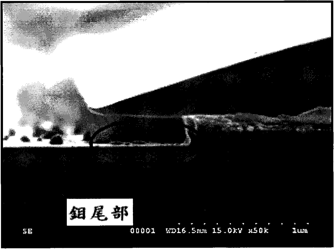
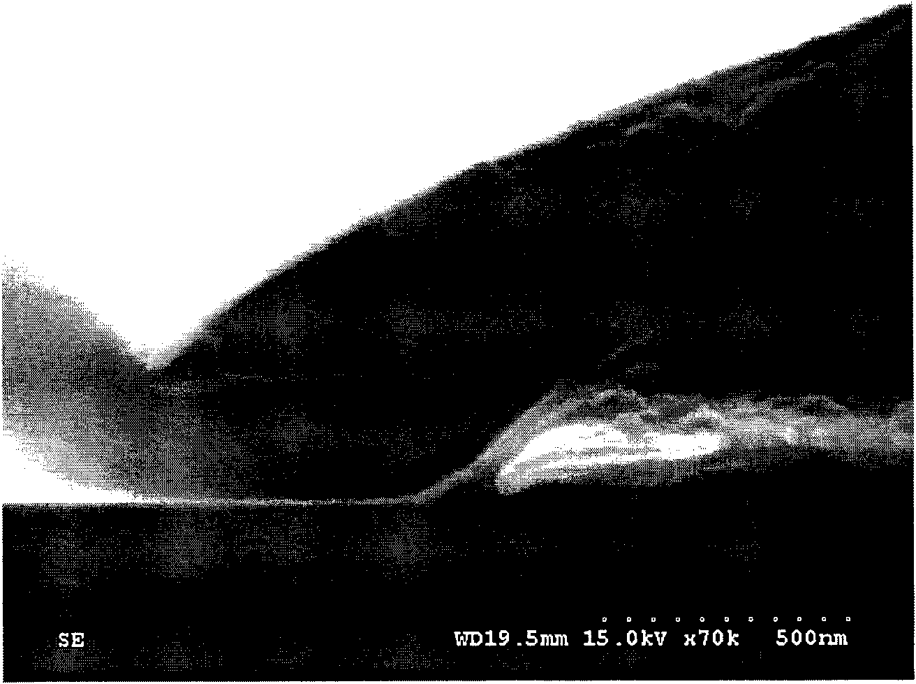
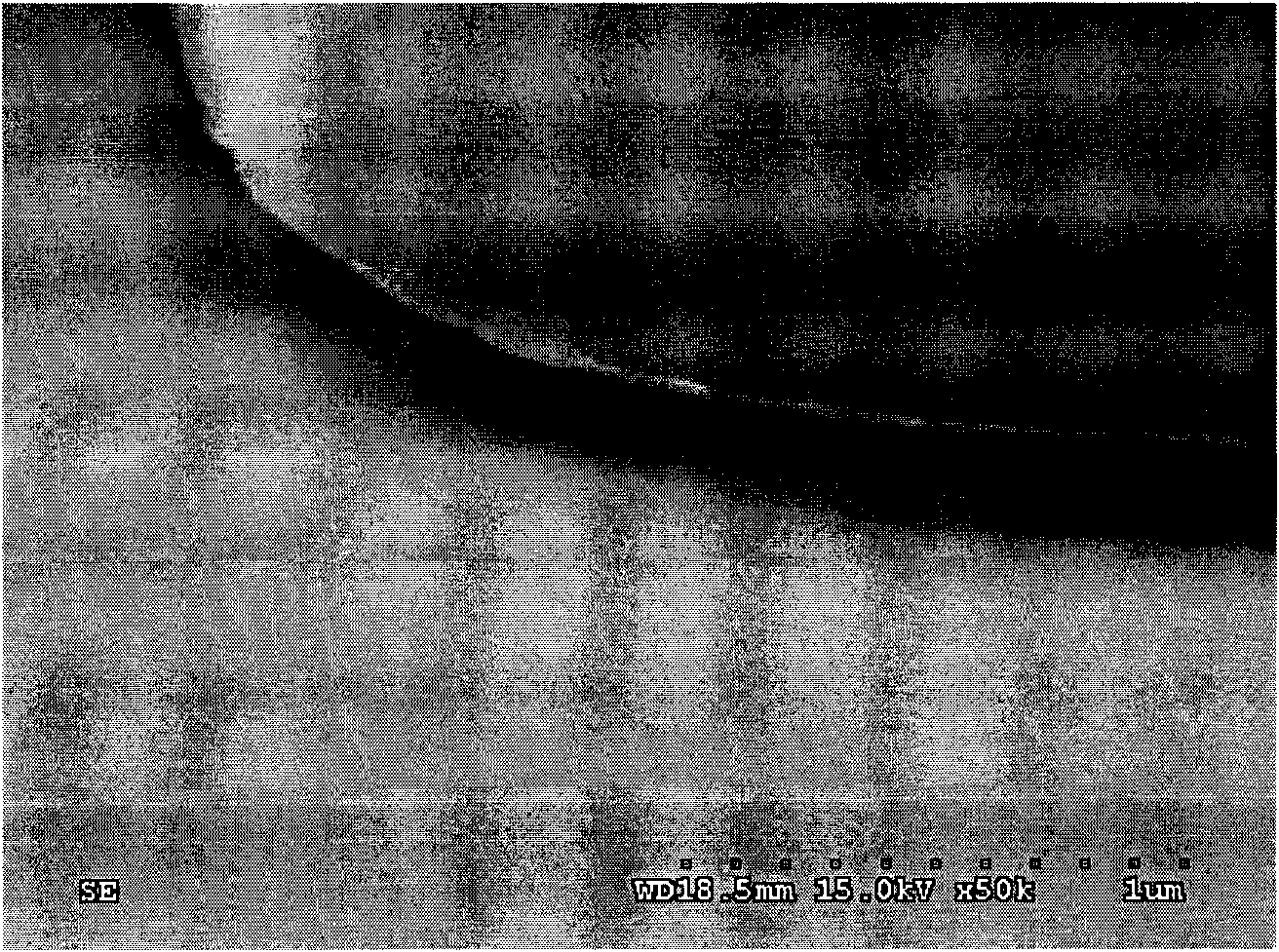
[0048] Hereinafter, the present invention will be described in detail with specific embodiments and comparative examples. The explanations described below are used to clearly understand the present invention, and are not intended to limit the scope of the present invention.

[0049] [Example and Comparative Example]

[0050] Prepare the etching solution

[0051] The etching solutions of the first to sixth examples and the first to fourth comparative examples were prepared by mixing the contents and components shown in Table 1 below.

[0052] etching method

[0053] Depositing a molybdenum layer (200 angstroms) on a glass substrate (100 mm x 100 mm), depositing a copper layer (1600 angstroms) on the molybdenum layer (200 angstroms), and forming a photoresist with a predetermined pattern through a photoresist process on the substrate. Then, an etching process was implemented on the copper / molybdenum double layer using the etching solutions of Examples 1-6 and Comparative Exa...


PUM


Abstract

The invention relates to a copper, copper/molybdenum, or copper/molybdenum alloy electrode etching solution, comprising: based on the total weight of the etching solution, 12-35 wt% of hydrogen peroxide, 0.5-5 wt% of sulfate, 0.5-5 wt% of phosphate, 0.0001-0.5 wt% of fluorine ion, 0.1-5 wt% of first water-soluble cyclic amine, 0.1-5 wt% of chelating agent, 0.1-5 wt% of second water-soluble cyclicamine, 0.1-5 wt% of diol, and deionized water, the total weight of the etching solution being 100 wt%. The invention relates to the copper, copper/molybdenum, or copper/molybdenum alloy electrode layer etching solution for use in the process of etching gate electrode, source electrode, or collecting electrode of the thin film transistor (TFT) in the liquid crystal display device or etching metallic wire.

Description

technical field [0001] The present invention relates to an etching solution for a copper (Cu) layer, a copper / molybdenum (Cu / Mo) layer, or a copper / molybdenum alloy (Cu / MoX) layer. Background technique [0002] In a semiconductor device, in order to form a metal line on a substrate, a process of forming a metal layer by sputtering, a process of forming a photoresist layer with a predetermined pattern on the metal layer, and using the photoresist as a contact window are generally performed. A contact mask is used to implement the etch process of etching. In particular, the etching process is performed by dry etching using such as plasma or wet etching using an etching solution. In the case of dry etching, since a high vacuum and the like are required, the etching conditions are strict and costly. Therefore, wet etching is more advantageous than dry etching when an appropriate etching solution is present. [0003] At the same time, in thin film transistor liquid crystal dis...

Claims


Application Information

Patent Timeline
IPC IPC(8): C23F1/14C23F1/18C23F1/30H01L21/28H01L21/3213G02F1/1362G02F1/1368
CPCC09K13/06C09K13/08C23F1/16C23F1/18C23F1/26
Inventor 李泰亨白贵宗
Owner SOULBRAIN CO LTD
Why Eureka
Try Eureka