

Method of flexibly connecting microelectrode array with printed circuit board (PCB)
A micro-electrode array, flexible connection technology, applied in contact parts, sensors, diagnostics, etc., can solve the problems of high cost of gold wire ball welding, inconvenient for operators to use repeatedly, and difficult to guarantee stability, and achieves high conductivity. Influence, shorten the production cycle, save the effect of production cost
- Summary
- Abstract
- Description
- Claims
- Application Information
AI Technical Summary
Problems solved by technology
Method used
Image

Examples
Embodiment Construction
[0029] In order to make the object, technical solution and advantages of the present invention clearer, the present invention will be described in further detail below in conjunction with specific embodiments and with reference to the accompanying drawings.
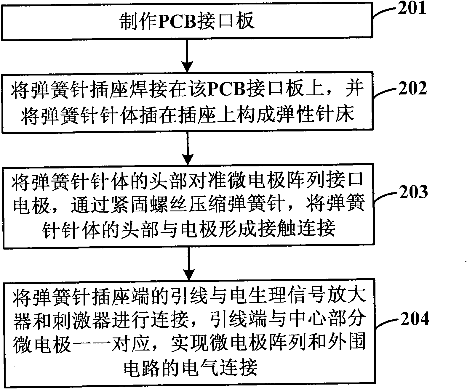
[0030] Such as figure 2 as shown, figure 2 It is a flow chart of a method for realizing the flexible connection between a microelectrode array and a PCB circuit provided by the present invention, and the method includes the following steps:
[0031] Step 201: making a PCB interface board;
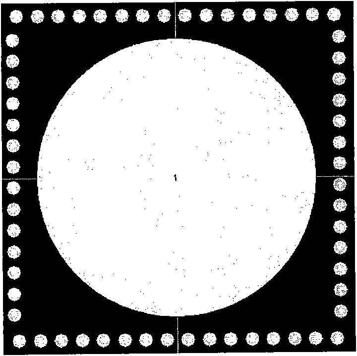
[0032] In this step, according to the size, gap and arrangement of the electrodes in the microelectrode array, a PCB interface board matching the electrodes is fabricated, and the pads of the interface board correspond to the electrodes one by one.
[0033] Step 202: Solder the pogo pin socket on the PCB interface board, and insert the pogo pin body into the socket to form an elastic needle bed, so that the pogo pin body is perpend...
PUM
 Abstract
Description
Claims
Application Information