Process for manufacturing 12OZ thick copper multilayer circuit board

A manufacturing process and circuit board technology, which is applied in the field of multilayer circuit board manufacturing process, can solve the problems of obvious barrier effect, uneven heat transfer, and affecting hole quality, so as to reduce side erosion effect, uniform pressure distribution, and improve etching factor effect

Active Publication Date: 2010-04-07
KALEX MULTI LAYER CIRCUIT BOARD (ZHONGSHAN) CO LTD
View PDF0 Cites 35 Cited by
  • Summary
  • Abstract
  • Description
  • Claims
  • Application Information

AI Technical Summary

Problems solved by technology

However, when the 12OZ thick copper plate is laminated on the inner layer, there is a large space to be filled with resin between the lines, and the line itself is thick, the barrier effect is obvious, which is not conducive to filling, and the number of layers is large, the heat transfer is uneven, and air bubbles and pressure are prone to occur. Bad fit etc.
[0005] The drilling process is to use a high-precision drilling machine to drill conduction holes and non-conduction holes on the pressed plate, and the connection between circuit layers and components an

Method used


Image

  • Process for manufacturing 12OZ thick copper multilayer circuit board
  • Process for manufacturing 12OZ thick copper multilayer circuit board
  • Process for manufacturing 12OZ thick copper multilayer circuit board

Examples


Embodiment

[0022] A manufacturing process of a 12OZ thick copper multilayer circuit board, including inner layer etching, pressing and drilling processes,

[0023] Among them, in the inner layer etching process, the CU in the acidic copper chloride etching solution is controlled 2+ The concentration is 150±20g / l, the temperature is 50±3℃, the total acidity is 2.8±.6N, the specific gravity is 1.30±0.10, the etching speed is 1.2±0.3m / min, the number of etching is 4 times, and the plate is turned over after each etching face once;

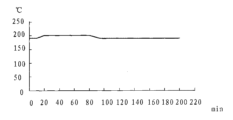
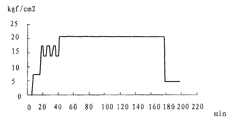
[0024] In the pressing process, it includes a hot pressing step and a cold pressing step, wherein the hot pressing time is 200min, the system is vacuumed and the absolute pressure is 10mbar between 5-95min, and the maximum pressure of the pressing plate is 21.42Kgf / cm 2 , the temperature is 190°C; the cold pressing time is 110min, and the maximum platen pressure is controlled at 18.36Kgf / cm 2 ;

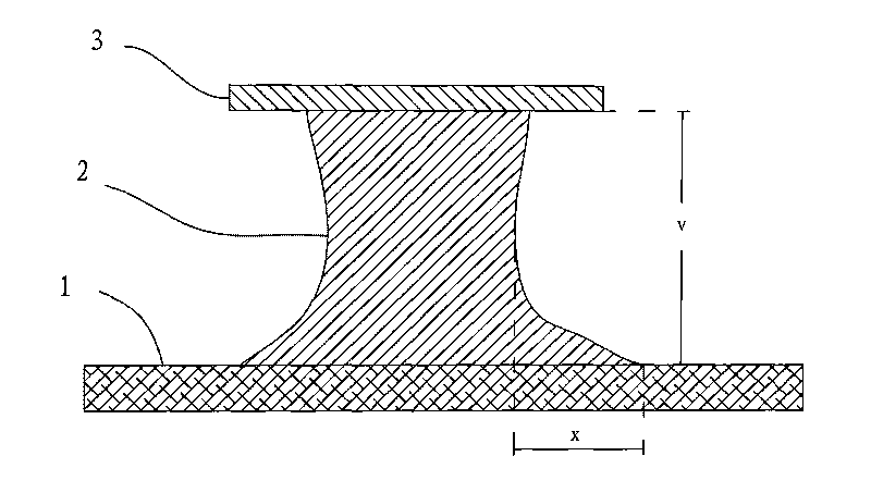
[0025] In the drilling process, when the diameter of the pre-dr...


PUM

PropertyMeasurementUnit
Peel strengthaaaaaaaaaa

Abstract

The invention discloses a process for manufacturing a 12OZ thick copper multilayer circuit board. In an inner layer etching process, the concentration of CU2+ in an acid copper chloride etching solution is controlled to be 150+/-20g/l, the temperature is 50+/-3 DEG C, total acidity is 2.8+/-0.6N, specific gravity is 1.30+/-0.10, etching speed is 1.2+/-m/min, and the number of etching times is 4 times; a plate pressing process comprises a hot pressing step and a cold pressing step, wherein the hot pressing time is 200 minutes, a system is vaccumized at absolute pressure of 10mbar between the fifth minute and the ninety-fifth minutes, the maximum press plate pressure is controlled to be 21.42Kgf/cm2, and the temperature is 190 DEG C; the time for cold pressing is 110 minutes, and the maximum press plate pressure is controlled to be 18.36Kgf/cm2; when the diameter D of a prebored hole is more than or equal to 2.0mm and is less than 4.8mm, a drill bit with diameter d of less than or equal to 1.7mm is used to prebore 4 holes, and the holes are redrilled by using a drill bit with the diameter D. The process has the advantages of improving the etching factors of the plate material of the inner layer, reducing the side etching effect with good plate pressing effect and protecting the bored holes from the phenomenon that the holes are blocked by copper scarp.

Description

technical field [0001] The invention relates to a manufacturing process of a copper circuit board, in particular to a manufacturing process of a multilayer circuit board. Background technique [0002] A circuit board is a board used to support electronic components and provide circuits to connect them. The circuit board from raw material to finished product shipment includes the following main processes: inner layer cutting, inner layer dry film, inner layer etching, inner layer automatic optical inspection, blackening, pressing plate, drilling, copper sinking, board surface plating, outer layer Dry film, circuit plating, outer layer etching, outer layer automatic optical inspection, wet green paint, white lettering, exterior processing, electrical testing, surface treatment, final inspection, packaging. 12OZ thick copper multilayer circuit board is used as an automotive electronic component, especially in the engine power supply part of the automotive central electrical po...

Claims


Application Information

Patent Timeline
IPC IPC(8): H05K3/46H05K3/00
Inventor 姜文东汤科文
Owner KALEX MULTI LAYER CIRCUIT BOARD (ZHONGSHAN) CO LTD
Why Eureka
Try Eureka