Cell electrofusion chip device based on columnar microelectrode array and electrofusion method

A microelectrode array and electrofusion technology, which is applied in the field of chips providing cell electrofusion and devices for biological cell electrofusion, can solve the problems of weak precise control of cells, large chip spacing, inability to achieve high-throughput fusion, etc. The effect of fusion efficiency

Inactive Publication Date: 2010-04-14
CHONGQING UNIV
View PDF1 Cites 36 Cited by
  • Summary
  • Abstract
  • Description
  • Claims
  • Application Information

AI Technical Summary

Problems solved by technology

[0007] However, traditional cell electrofusion equipment also has some disadvantages: (1) Due to the large electrode spacing in the fusion tank, a high external driving voltage is required to achieve sufficient strength of cell queuing, fusion and compaction signals, often as high as Hundreds of thousands of volts, high requirements on the electrical safety of the system, the cost of the system is also greatly increased; (2) The large distance between electrodes is not conducive to the precise control of cells, etc.
[0010] However, there are still some problems with the above-mentioned chips. For example, although the microfluidic chip researched by MIT in the United States has solved the problem of cell pairing, the distance between the two electrodes of the chip is relatively large, and a high external voltage is still required. capable of electrofusion
However, Zhao Zhiqiang proposed that the number of microelectrodes integrated on the chip is small, and high-throughput fusion cannot be achieved; the electric field strength and electric field gradient generated by the microelectrodes are relatively weak, which is relatively weak in terms of precise control of cells; in terms of the selection of processing materials, corrosion resistance, The anti-oxidation ability is also weak; in addition, because the chip uses a planar two-dimensional microelectrode array, there is a great risk of clogging when the cells flow inside the chip; at the same time, because the sample inlet and outlet device is not integrated, the operation is also inconvenient
The method proposed by Japanese researchers is inefficient, and the fusion flux is far from enough to meet the research requirements of fused cells

Method used


Image

  • Cell electrofusion chip device based on columnar microelectrode array and electrofusion method
  • Cell electrofusion chip device based on columnar microelectrode array and electrofusion method
  • Cell electrofusion chip device based on columnar microelectrode array and electrofusion method

Examples


Embodiment 1

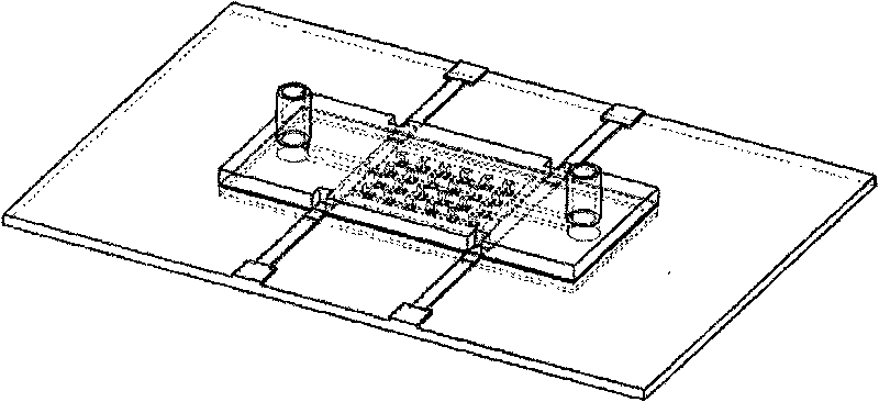
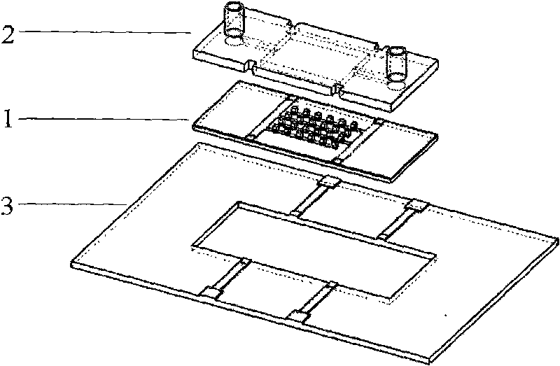
[0053] see figure 1 with figure 2 , the cell electrofusion chip device based on a columnar microelectrode array is composed of a columnar microelectrode array chip 1 , a flow path control module 2 and a peripheral printed circuit board 3 .

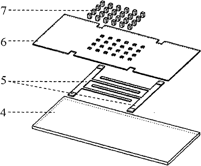
[0054] see image 3 The micro-chamber array chip 1 is composed of a quartz base layer 4, a metal wire layer 5, a polymer insulating layer 6 and a columnar micro-electrode array layer 7 in sequence from bottom to top.

[0055] see Figure 4 , the metal wire layer 5 is built on the quartz base layer 4 by micromachining technology, and is a staggered comb-shaped lead array. The material is selected from metals such as aluminum and copper with good conductivity, and the thickness is 1-3 μm. The comb-shaped lead array of the comb The width of the ridge 9 can be wider and can be controlled within the range of 100-500 μm to ensure good conductivity and reliability; the width of the comb teeth 10 is determined according to the density of the m...

Embodiment 2

[0061] Embodiment 2: the processing of each part of this device:

[0062] 1. The columnar microelectrode array chip is realized by MEMS processing technology, and the processing steps are as follows (the metal array electrode layer material described here is gold Au, and the polymer layer material is polyimide):

[0063] A. Use quartz as the substrate for processing chips;

[0064] B. Build a layer of aluminum on the quartz substrate with a thickness of 1-3 μm;

[0065] C. A comb-shaped microarray structure can be formed on the aluminum layer by photolithography to form a metal wire layer;

[0066] D. Spin-coat polyimide glue on the surface of the above structure to form a polyimide insulating layer with a thickness of 3-5 μm;

[0067] E. Photoetching polyimide to form micropores;

[0068] F. Sputter a layer of Ti / W on the aluminum surface where the photolithographic microholes are exposed, with a thickness of 50nm;

[0069] G. Electroplate a layer of gold on the surface o...

Embodiment 3

[0078] Embodiment 3: continuous flow fusion method

[0079] From the sample inlet 18 described in embodiment 1, use micropump to inject cell suspension; The wide space of the electrode array can make the cells flow freely; the sine wave electric stimulation signal is applied to the metal wire layer 5 through the peripheral printed circuit board 3, and a non-uniform gradient electric field will be formed between the opposite columnar microelectrodes, and the two electrodes between the microelectrodes Each cell will be lined up under the action of dielectrophoretic force; after the queuing is completed, a square wave pulse sequence signal is applied, and the cell pair that has completed the queuing will complete cell electroporation-cell electrofusion under the action of a high-intensity pulsed electric field between the microelectrodes Wait for the process. After the cell electrofusion process is completed, combined with the flow control device 2, the micropump is used to inje...


PUM

PropertyMeasurementUnit
thicknessaaaaaaaaaa
thicknessaaaaaaaaaa
thicknessaaaaaaaaaa

Abstract

The invention provides a cell electrofusion chip device based on a columnar microelectrode array, which consists of a columnar microelectrode array chip, a printed circuit board and a flow passage control module. The columnar microelectrode array chip consists of a quartz substrate layer, a metal lead layer, a polymer insulated layer and a columnar microelectrode layer sequentially from bottom to top, wherein the metal lead layers of the columnar microelectrode array chip is electrically connected with the periphery printed circuit board in a bonding way, leads outside electrical signals onto a columnar microelectrode, and leads a gradient electric field with enough strength to be formed between adjacent columnar microelectrodes; and the flow passage control module covers the columnar microelectrode array chip. In the invention, by loading electrical signals on the columnar microelectrode, queue and fusion among cells are controlled; simultaneously, the superiority that the columnar microelectrode array benefits the flow of the cells in chamber-tracts is utilized for realizing continuous stream fusion of the cells; and with the combination of the design of the array columnar microelectrode, the continuous, high-efficient and high-throughput fusion of the cells in the device is realized.

Description

technical field [0001] The invention relates to a device for electrical fusion of biological cells. Specifically, the present invention relates to a chip for providing cell electrofusion, providing and generating the electric field intensity and electric field gradient required for cell alignment, electroporation, and fusion. The patent of the invention relates to the precise control of cells in cell electrofusion and the high-efficiency fusion of cells, and is applicable to genetics, animal and plant distant hybridization breeding, developmental biology, drug screening, monoclonal antibody preparation, mammalian cloning and other fields. Background technique [0002] Since the 1980s, cell electrofusion technology has been rapidly developed and widely used because of its high efficiency, simple operation, non-toxicity to cells, easy observation, suitable for instrument application and standardized operation. [0003] Cell electrofusion can be divided into two stages: cell q...

Claims


Application Information

Patent Timeline
Patent Type & Authority Applications(China)
IPC IPC(8): C12M1/42C12N15/02
CPCC12M35/02
Inventor 胡宁杨军郑小林胡南夏斌蒋凤赵丽苹刘琳琳田浩张小玲
Owner CHONGQING UNIV
Why Eureka
Try Eureka