Micro reflector array manufacturing method

A technology of a micro-mirror array and a manufacturing method, which is applied in the field of manufacturing large arrays, micro-mirror arrays with high fill factor, and large-angle twist fields, and can solve the problems of low fill factor, small twist angle, and high fill factor of mirrors.

Active Publication Date: 2010-06-02
THE 13TH RES INST OF CHINA ELECTRONICS TECH GRP CORP
View PDF0 Cites 20 Cited by
  • Summary
  • Abstract
  • Description
  • Claims
  • Application Information

AI Technical Summary

Problems solved by technology

[0009] The technical problem to be solved by the present invention is to provide a method for manufacturing micro-mirror arrays to solve the problems of low filling factor, sma

Method used


Image

  • Micro reflector array manufacturing method
  • Micro reflector array manufacturing method
  • Micro reflector array manufacturing method

Examples


Example Embodiment

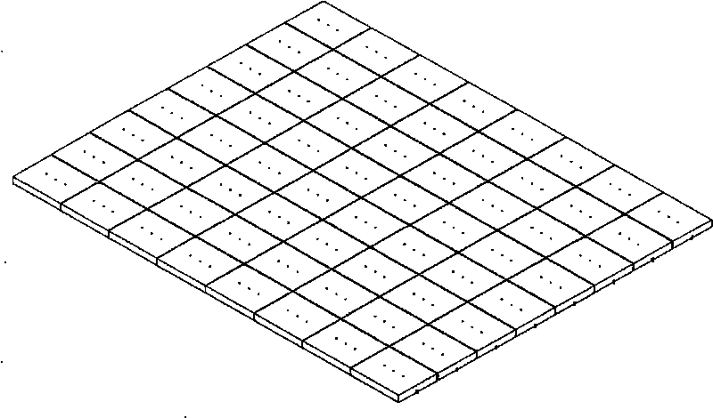
[0034] image 3 It is a top view of a unit in the micromirror array. The material of the mirror surface is a silicon polished surface. The smooth silicon surface has a high reflectivity to reduce the reflection loss of light. The surface of the mirror has a support post release hole.

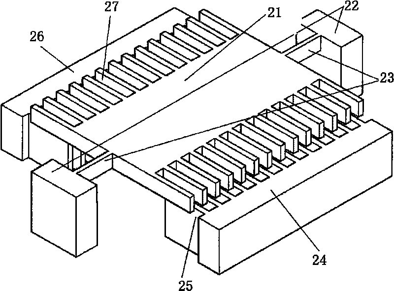
[0035] Figure 4 It is a cross-sectional view of a unit in the micromirror array, which is bonded together by a substrate glass sheet 1, a driving structure layer silicon sheet 2, and a mirror surface layer silicon sheet 3 through a wafer bonding process, including a moving drive comb 4, a reflector Mirror surface 5, bonding metal layer (moving tooth drive electrode) 6, release hole 7, twist beam 8, fixed tooth drive electrode (1) 9, fixed drive comb teeth 10, support column (after release) 11, fixed tooth drive electrode (2) 12, wherein there are metal wirings on the surface of the glass substrate 1 and the silicon wafer 2 of the driving structure layer. Its working principle is: the fixed dr...


PUM

PropertyMeasurementUnit
Thicknessaaaaaaaaaa
Thicknessaaaaaaaaaa
Thicknessaaaaaaaaaa

Abstract

The invention discloses a micro reflector array manufacturing method which is used for manufacturing micro reflector array with high fill factors, big-angle torsion and big array. The method adopts bulk-silicon MEMS processing technology, a vertical comb driving mode, wafer bonding technology and etching technology and is characterized in that the wafer is bonded after a middle driver layer is processed, a layer of reflector surface is covered above the driver layer; on the basis, a special deep etching release technology is adopted to release a shore reserved in the driver layer to realize micro reflector torsion, thus realizing the purpose of driving with high fill factors, big-angle torsion and low voltage.

Description

technical field [0001] The invention relates to a method for manufacturing a microreflector array, which is especially suitable for manufacturing a microreflector array with large array, large-angle twist and high filling factor. Background technique [0002] MOEMS (Micro-Optical Electro-Mechanical System) is an integrated system of light, machinery and electricity. With the development of information technology and optical fiber communication technology, MOEMS has become a current research hotspot. Adaptive optics and optical sensing and many other aspects. The new type of optical device manufactured by MEMS technology has small insertion loss, extremely low crosstalk between optical paths, is insensitive to the wavelength and polarization of light, and usually uses silicon as the main material, so the optical, mechanical and electrical properties of the device are excellent. [0003] The core component to change the direction of "light" in MOEMS is the mirror. With the ra...

Claims


Application Information

Patent Timeline
IPC IPC(8): G02B26/08
Inventor 徐永青杨拥军李艳丽
Owner THE 13TH RES INST OF CHINA ELECTRONICS TECH GRP CORP
Why Eureka
Try Eureka