Method and system for exchanging two silicon wafer stages of photoetching machine

A technology for exchanging systems and wafer stages, which is applied in the field of high-efficiency lithography machine dual wafer stage exchanging systems, can solve the problems of insufficient space utilization, processing and assembly accuracy, and shorten exchange time, reduce installation accuracy requirements, The effect of improving system efficiency and space utilization

Active Publication Date: 2011-05-11
TSINGHUA UNIV +1
View PDF4 Cites 2 Cited by
  • Summary
  • Abstract
  • Description
  • Claims
  • Application Information

AI Technical Summary

Problems solved by technology

[0008] Aiming at the deficiencies and defects of the silicon wafer table technology of the existing lithography machine, the present invention proposes a new high-efficiency, simple structure, high exchange efficiency, high space utilization rate, and no collision between linear guide rails during exchange. The dual-silicon wafer stage exchange system of the lithography machine can overcome the shortcomings of the existing dual-silicon wafer stage exchange system, such as non-centroid drive, insufficient space utilization, and extremely high processing and assembly precision requirements, so that it has a simple structure and space utilization. The advantages of high efficiency and no collision between linear guide rails during exchange can further improve the exchange efficiency and exposure efficiency of the lithography machine

Method used


Image

  • Method and system for exchanging two silicon wafer stages of photoetching machine
  • Method and system for exchanging two silicon wafer stages of photoetching machine
  • Method and system for exchanging two silicon wafer stages of photoetching machine

Examples


Embodiment Construction

[0026] Below in conjunction with accompanying drawing, structure, principle and working process of the present invention are described further

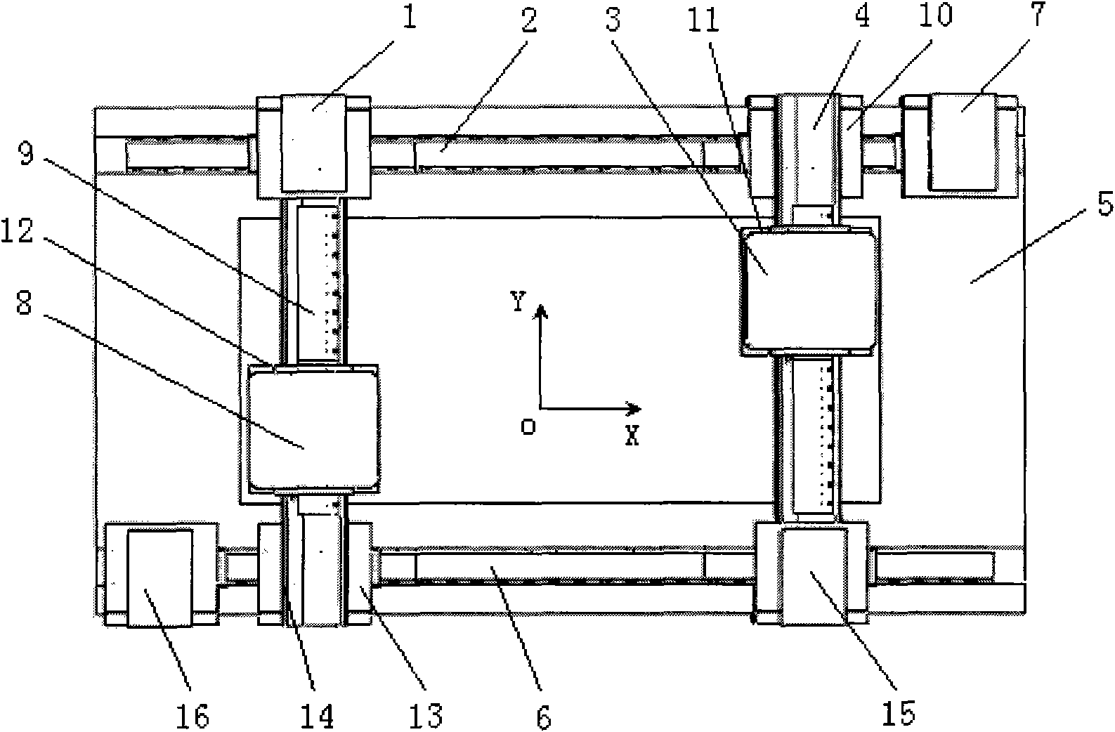
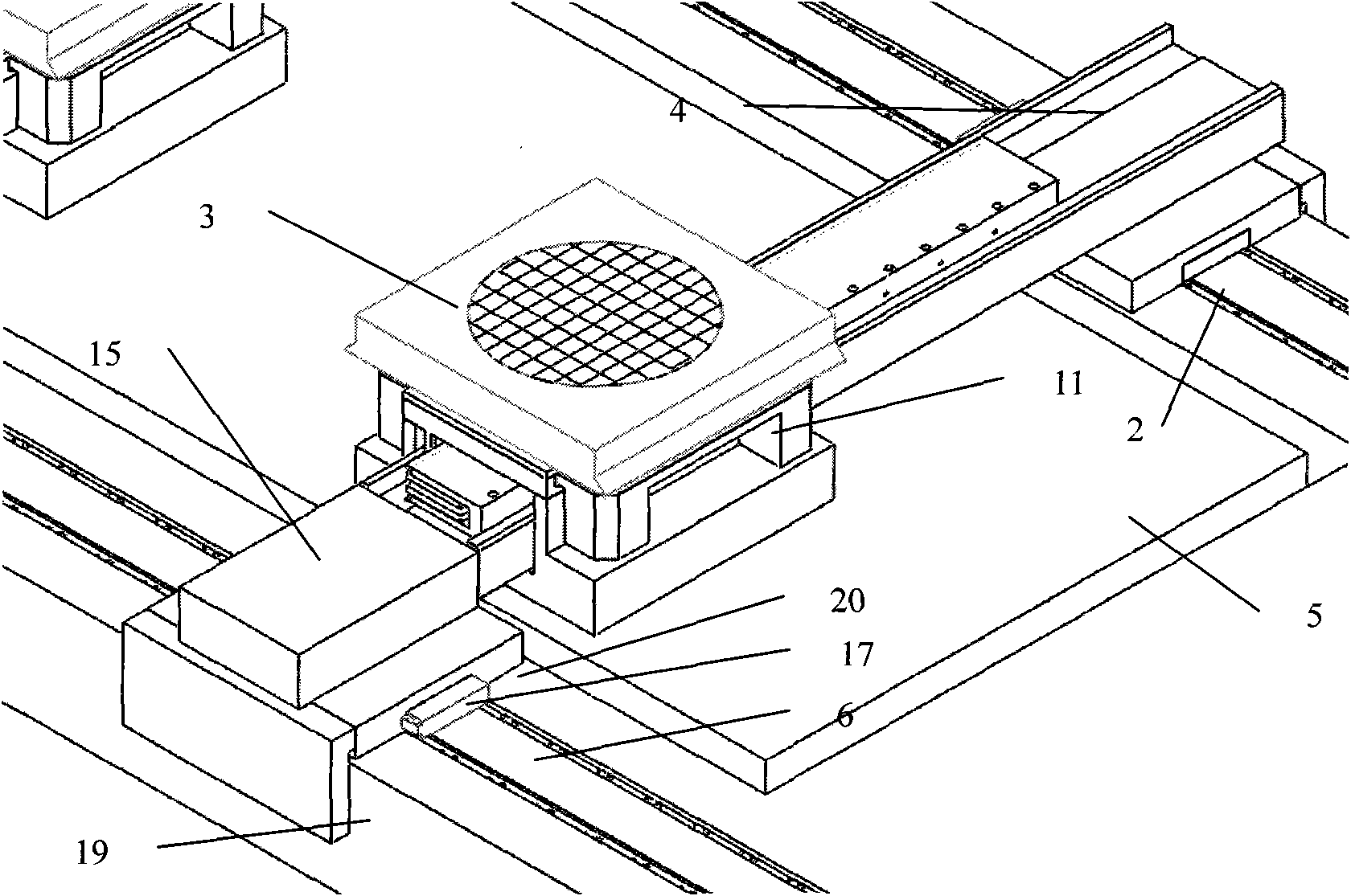
[0027] figure 2 Schematic diagram of the structure of the dual-wafer stage exchange system of the lithography machine provided by the present invention, the system includes the first wafer stage 3 operating at the exposure station, the second wafer stage 8 operating at the pre-processing station, the first X-direction linear guide rail 2, second X-direction linear guide rail 6, first single-degree-of-freedom auxiliary drive unit 1, second single-degree-of-freedom auxiliary drive unit 7, third single-degree-of-freedom auxiliary drive unit 15, fourth single-degree-of-freedom auxiliary drive unit Drive unit 16, first Y-direction guide rail 4, second Y-direction guide rail 9, first wafer stage auxiliary drive unit 11, second wafer stage auxiliary drive unit 12, first main drive unit 10, second main drive unit 13 and the base 5, the long...


PUM


Abstract

The invention discloses of a method and a system for exchanging two silicon wafer stages of a photoetching machine. The system comprises a base station, two silicon wafer stages, two linear guide rails in an X direction, two linear guide rails in a Y direction, two auxiliary drive units for the silicon wafer stages and four unidirectional auxiliary drive units; the system also comprises two master drive units by which the guide rails in the Y direction can be driven to move along the X direction and rotate in the plane of the base station; when rotating to not interfere with each other along the X direction, the two guide rails in the Y direction take the silicon wafer stages to move face to face along the X direction, when changing from the face-to-face movement into the reverse movement, the two guide rails in the Y direction rotate oppositely to realize the position exchange of the two silicon wafer stages. Through the simultaneous rotation of two guide rails, the system saves the time for exchanging the two silicon wafer stages, simplifies the system structure, improves the efficiency and the space use ratio as well as the precision of the system, and overcomes the shortcomings of accordant size of the silicon wafer stage, high precision requirement on part processing and assembling and the like.

Description

technical field [0001] The invention relates to a high-efficiency dual-silicon wafer platform exchange system for photolithography machines. The system is applied to semiconductor photolithography machines and belongs to the technical field of semiconductor manufacturing equipment. Background technique [0002] In the production process of integrated circuit chips, the exposure transfer (photolithography) of the design pattern of the chip on the photoresist on the surface of the silicon wafer is one of the most important processes. The equipment used in this process is called a photolithography machine (exposure machine). The resolution and exposure efficiency of the lithography machine greatly affect the characteristic line width (resolution) and productivity of the integrated circuit chip. As the key system of the lithography machine, the motion accuracy and work efficiency of the silicon wafer ultra-precision motion positioning system (hereinafter referred to as the wafe...

Claims


Application Information

Patent Timeline
Patent Type & Authority Patents(China)
IPC IPC(8): G03F7/20
CPCH01L21/68G03F7/70725G03F7/70733G03F7/70758
Inventor 朱煜张鸣徐登峰汪劲松董立立杨开明尹文生胡金春许岩马竞田丽李玉洁王婧
Owner TSINGHUA UNIV
Why Eureka
Try Eureka