Protective film forming method and apparatus

A technology of covering device and film, which is applied in the manufacture of devices, electrical components, and semiconductor/solid-state devices that apply liquid to the surface. The amount of use, good affinity, and the effect of increasing the ratio

Active Publication Date: 2010-06-16
DISCO CORP
View PDF2 Cites 10 Cited by
  • Summary
  • Abstract
  • Description
  • Claims
  • Application Information

AI Technical Summary

Problems solved by technology

However, when laser light is irradiated along the interval lanes of the wafer, a new problem occurs as follows: heat energy is concentrated on the irradiated area to generate debris, which adheres to the pads connected to the circuit ( bonding pad) and so on to reduce the quality of the chip
However, the affinity between liquid resins such as polyvinyl alcohol and the wafer is low, so areas not covered with the protective film are scattered locally, and it is difficult to cover the surface of the wafer with a protective film of uniform thickness.
Therefore, since the rotary table rotates at a high speed of, for example, 3000 rpm as described above, 99% of the liquid resin dripped onto the wafer surface is scattered and discarded.

Method used


Image

  • Protective film forming method and apparatus
  • Protective film forming method and apparatus
  • Protective film forming method and apparatus

Examples


Embodiment Construction

[0032] Hereinafter, preferred embodiments of the protective film covering method and protective film covering apparatus according to the present invention will be described in detail with reference to the accompanying drawings.

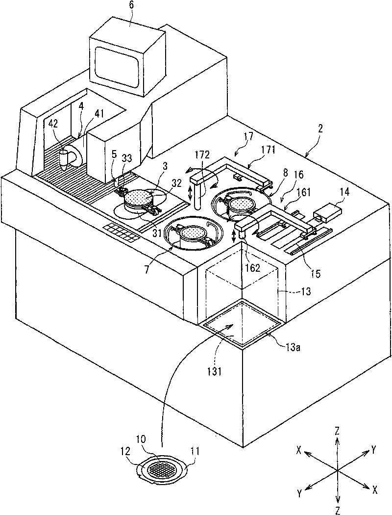
[0033] exist figure 1 , shows a perspective view of a laser processing machine equipped with a protective film covering device according to the present invention.

[0034] figure 1 The laser processing machine shown has an approximately cuboid housing 2 . In the casing 2 of this device, a chuck table 3 as a workpiece holding unit for holding a workpiece is disposed so as to be movable in a direction indicated by an arrow X which is a machining feeding direction. The chuck table 3 has a suction chuck support base 31 and a suction chuck 32 mounted on the suction chuck support base 31, and sucks, for example, a disc-shaped semiconductor to be processed by a suction unit not shown. The wafer is held on the surface of the suction chuck 32 , that is, the m...


PUM


Abstract

A protective film forming method for forming a protective film of resin on a work surface of a wafer. The protective film forming method includes a wafer holding step of holding the wafer on a spinner table in the condition where the work surface is oriented upward, a spray coating step of spraying first liquid resin onto the work surface of the wafer as rotating the spinner table at a first rotational speed after performing the wafer holding step, a liquid resin supplying step of dropping a predetermined amount of second liquid resin onto a central area of the work surface of the wafer as rotating the spinner table at a second rotational speed lower than the first rotational speed after performing the spray coating step, and a spin coating step of rotating the spinner table at a third rotational speed higher than the first rotational speed after performing the liquid resin supplying step to thereby spread the second liquid resin dropped onto the central area of the work surface of the wafer, thus forming the protective film on the work surface of the wafer.

Description

technical field [0001] The present invention relates to a method and a device for covering a resin protective film on the surface of a wafer such as a semiconductor wafer or an optical device wafer. Background technique [0002] In the manufacturing process of a semiconductor device, a plurality of regions are divided on the surface of a generally disc-shaped semiconductor wafer by dividing lines called streets arranged in a grid pattern, and IC (integrated wafers) are formed in the divided regions. circuit: integrated circuit), LSI (large-scale integration: large-scale integrated circuit), liquid crystal driver, flash memory and other devices. Then, the region where the devices are formed is divided by cutting the semiconductor wafer along the lanes, thereby manufacturing individual devices. Alternatively, the surface of the optical device wafer is divided into a plurality of regions by grid-shaped streets on the surface of a sapphire substrate or the like, and optical dev...

Claims


Application Information

Patent Timeline
Patent Type & Authority Applications(China)
IPC IPC(8): H01L21/56H01L21/00B05D1/36
CPCH01L21/68728H01L21/68785H01L21/6715
Inventor 北原信康远藤智章芥川幸人
Owner DISCO CORP
Why Eureka
Try Eureka