

ZnO nanosphere-based GaN-based light emitting diode surface roughening method
A technology of light-emitting diodes and surface roughening, which is applied to electrical components, circuits, semiconductor devices, etc., can solve the problems of reduced light-emitting area, reduced luminous efficiency, and unstable process. It is easy to achieve size, improve extraction efficiency, and simple process Effect
- Summary
- Abstract
- Description
- Claims
- Application Information
AI Technical Summary
Problems solved by technology
Method used
Image

Examples
Embodiment Construction
[0028] The present invention will be further described below in conjunction with the accompanying drawings and embodiments.
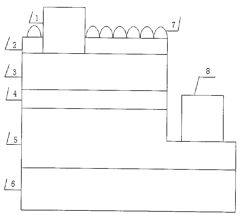
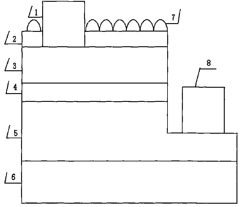
[0029] figure 2 Marking description in: 1-P pad, 2-transparent P-type electrode, 3-P-type GaN material, 4-quantum well, 5-N-type GaN material, 6-substrate, 7-nanometer ZnO roughening layer , 8-N pressure solder joints.
[0030] The GaN-based light-emitting diode whose surface is roughened with ZnO nanospheres sequentially includes: a substrate, a GaN-based epitaxial layer, a transparent electrode on a P-type material for ohmic contact, ZnO nanospheres, and P and N pressure solder joints.
[0031] Wherein, the substrate may be sapphire, silicon carbide, or silicon.
[0032] Wherein, the GaN-based epitaxial layer includes N-type material, quantum well, and P-type material.
[0033] Wherein, the P-type transparent electrode can be a metal material or an oxide material, and the metal material is: Pd, Au or NiAu; the oxide material is ZnO, NiO mgO, In2O3...
PUM
 Abstract
Description
Claims
Application Information