Processing technology of printed circuit board

A technology of printed circuit board and processing technology, which is applied in the directions of secondary processing of printed circuit, multi-layer circuit manufacturing, coating of non-metallic protective layer, etc., which can solve the problems of damaging the solder mask layer, time-consuming and laborious, etc.

Active Publication Date: 2010-06-30
SHENNAN CIRCUITS
View PDF0 Cites 15 Cited by
  • Summary
  • Abstract
  • Description
  • Claims
  • Application Information

AI Technical Summary

Problems solved by technology

This method has an obvious disadvantage, because the solder resist will expand and overflow the via hole when it is heated and solidified, so that the periphery of the via hole will also be covered with solder resist. When the part of the solder resist) is very close, or when the via hole itself needs to be opened on one side, the solder resist will overflow and cover the board surface that does not need to cover the solder resist. At this time, these overflow solder resist must be carefully removed. It is very time-consuming and labor-intensive, and it is easy to damage the solder mask layer of the outer layer circuit or other parts that have been made when removing the spilled solder mask

Method used


Image

  • Processing technology of printed circuit board
  • Processing technology of printed circuit board

Examples


Embodiment 1

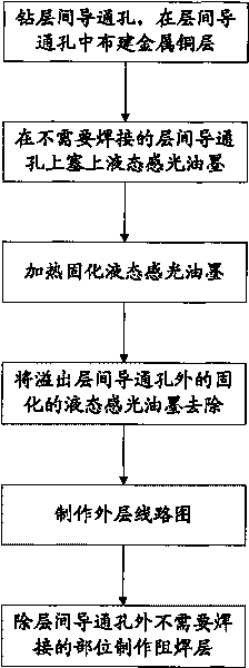
[0024] see figure 1 As shown in the process, this embodiment provides a printed circuit board processing technology, and the printed circuit board processing technology includes the following steps in sequence:

[0025] A. Drill via holes, and build a metal copper layer in the via holes. The specific order is: drilling, bulking, holeization, copper sinking, degreasing, pickling, and copper plating;

[0026] B. Plug liquid photosensitive ink on the via holes that do not need to be soldered. The specific order is as follows: Prepare an aluminum plate with holes. The holes on the aluminum plate correspond to the holes that need to be plugged in the circuit design. Cover the aluminum plate to the circuit. Align the corresponding holes on the board, and use silk screen printing to plug the via holes with ink;

[0027] C. Heating and curing the liquid photosensitive ink in the via hole; specifically: first use 80°C to heat the solder resist in the via hole for 60 minutes, then use ...

Embodiment 2

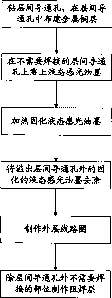
[0034] This embodiment provides a printed circuit board processing technology, which sequentially includes the following steps:

[0035] A. Drill via holes, and build a metal copper layer in the via holes, the specific order is: drilling, sinking copper, and copper plating;

[0036] B. Make the outer layer circuit, specifically in order: film sticking, exposure and development, and copper etching.

[0037] C. Plug liquid photosensitive ink on the via holes that do not need to be soldered, and use a small hollow tube to pour photosensitive ink into each via hole that needs to be plugged;

[0038] D. Heating and curing the liquid photosensitive ink in the via hole; specifically: heating the solder resist in the via hole at 150°C for 60 minutes;

[0039] E. Shovel and scrape off the solidified liquid photosensitive ink overflowing the via hole; the specific sequence is: use a 600-mesh brush roller grinding plate;

[0040] F. Make a liquid photosensitive ink solder resist layer ...


PUM


Abstract

The invention discloses a processing technology of a printed circuit board, sequentially comprising the following steps of: drilling a conducting hole and establishing a metal copper layer in the conducting hole; stuffing a solder mask in the conducting hole with no need for welding; heating and solidifying the solder mask in the conducting hole; removing the solidified solder mask overflowing out of the conducting hole; and making a solder mask layer in the positions of the printed circuit board except for the conducting hole with no need for welding. The invention solves the processing problem that the solder mask overflows and covers plate faces without being covered by the solder mask to be inconvenient to remove when the conducting hole is near to a windowing part with the need for welding or when the conducting hole needs single-face windowing. The processing technology of the printed circuit board can be used for accurately making the conducting hole and the solder mask layer with low cost without affecting the making effect of the solder mask layers of other parts.

Description

technical field [0001] The invention relates to a processing technology of a printed circuit board, in particular to a processing technology of a multilayer printed circuit board. Background technique [0002] After the outer circuit is completed, the multilayer printed circuit board needs to be coated with an insulating resin layer to protect the circuit and avoid oxidation and soldering short circuit. Before coating, it is usually necessary to roughen and clean the copper surface of the circuit board by brushing, micro-etching, etc., and then apply liquid photosensitive ink to the board surface by screen printing, curtain coating, electrostatic spraying, etc. Then pre-dry it (the dry film photosensitive green paint is pressed and coated on the board surface with a vacuum laminating machine). After it is cooled, it is sent to an ultraviolet exposure machine for exposure. After the green paint is irradiated by ultraviolet rays in the light-transmitting area of ​​the film, a...

Claims


Application Information

Patent Timeline
Patent Type & Authority Applications(China)
IPC IPC(8): H05K3/28H05K3/46
Inventor 张春林刘宝林罗斌
Owner SHENNAN CIRCUITS
Why Eureka
Try Eureka