Magnetic random access memory, magnetic logic device and spinning microwave oscillator

A random access memory, magnetic technology, applied in static memory, digital memory information, information storage and other directions, can solve the problems of large trigger current, low power consumption, unfavorable application and development of low-power devices, and limited application scope.

Active Publication Date: 2010-07-07
INST OF PHYSICS - CHINESE ACAD OF SCI
View PDF1 Cites 23 Cited by
  • Summary
  • Abstract
  • Description
  • Claims
  • Application Information

AI Technical Summary

Problems solved by technology

However, in order for the latter to realize the direct current reversal of the magnetic moment, it needs to be as high as 1×10 12 A / m 2 Write current density, although people have reduced the write current density by adopting a ring-shaped memory cell design (see patent application CN1901088), that is, to 1×10 10 A / m 2 , but this magnitude is still very large, which is very unfavorable for the application development of low-power and low-power devices in the future; and when the writing current density of high current density flows through the device, the device structure is easily damaged under high current density. Destruction, affecting the service life of the device under repeated reading and writing also has a great impact
Similarly, in existing spin microwave oscillators (see patent application 200810222965), the trigger current required to achieve magnetic moment precession is usually very large, which also limits the application of the device
Furthermore, similar magnetic logic devices (see patent application PCT / CN2007 / 001174) are also affected by high current density logic inputs, thereby limiting their application range

Method used


Image

  • Magnetic random access memory, magnetic logic device and spinning microwave oscillator
  • Magnetic random access memory, magnetic logic device and spinning microwave oscillator
  • Magnetic random access memory, magnetic logic device and spinning microwave oscillator

Examples


Embodiment 1

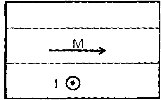
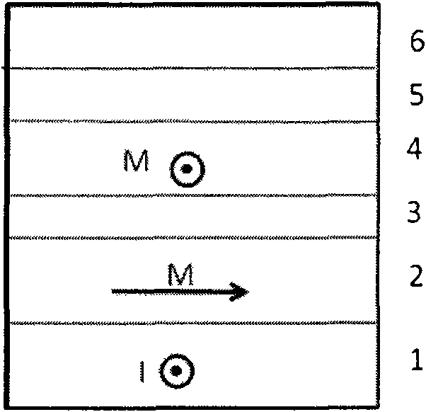
[0089] Figure 2B It is a cross-sectional view of a magnetic random access memory cell (MRAM cell) using the above-mentioned magnetic multilayer film memory cell with the Rashba effect according to Embodiment 1 of the present invention. It can be seen from the figure that the entire MRAM cell includes layers 1a, 1b, 1c, 1d, 1e, 1f, 1g, and the non-functional regions in these layers are made of insulating buried dielectric such as SiO 2 etc. buried, wherein the metal wiring layer has three layers, that is, the layer 1d where the read bit line BL14c is located, the layer 1f where the write bit line BL24d is located, and the layer 1b where the ground line GND 4a and the transition metal layer TM 4b are located. Wherein, the two bit lines BL14c and BL24d are respectively arranged above the magnetic multilayer memory unit ML 6 , are separated from each other by an insulating layer 1e, and are perpendicular to the word line 2 . The magnetic multilayer film memory cell ML6 is arrang...

Embodiment 2

[0095] The MRAM unit was manufactured in the same manner as in Example 1, except for the magnetic multilayer memory unit. The magnetic multilayer film storage unit is: in Si / SiO 2 On the substrate, the non-magnetic layer Pt (1-5nm) and the ferromagnetic layer LaSrMnO are grown sequentially. x (3~5nm), then grow the intermediate layer CaMnO (1~2nm), the pinned ferromagnetic layer CoFe (2~5nm), the antiferromagnetic pinning layer IrMn (10nm), and the covering layer Ta (5nm); the magnetic The cross section of the multilayer film memory unit is a rectangular ring, the inner ring width of the rectangular ring is 50000nm, the ring width is 1000nm, and the ratio of the inner ring width to the length is 1:5.

Embodiment 3

[0097] The MRAM unit was manufactured in the same manner as in Example 1, except for the magnetic multilayer memory unit. The magnetic multilayer film storage unit is: firstly, in Si / SiO 2 On the substrate, the non-magnetic layer Pt (1-5nm) and the ferromagnetic layer GaMnAs (3-5nm) are grown sequentially, and then the intermediate layer CaAs (1-2nm) is grown, and the ferromagnetic layer CoFe (2-5nm) is pinned. The ferromagnetic pinning layer IrMn (10nm), the covering layer Ta (5nm), the cross section of the magnetic multilayer film storage unit is circular, and its diameter is 10000nm.


PUM

PropertyMeasurementUnit
thicknessaaaaaaaaaa
thicknessaaaaaaaaaa
widthaaaaaaaaaa

Abstract

The invention discloses a magnetic random access memory unit based on Rashba effect. The magnetic random access memory unit comprises a magnetic multilayer film memory unit and a bit-writing line. The magnetic random access memory unit is characterized in that the magnetic multilayer film memory unit comprises a substrate, a non-magnetic layer, a core functional layer zone and a covering layer from bottom to top; the core functional layer zone comprises a lower magnetic layer, a medium layer and a upper magnetic layer from bottom to top; the bit-writing line is connected with the non-magneticlayer so that write current flows through the non-magnetic layer transversely and the magnetic torque of the lower magnetic layer is reversed, thus writing data. The invention also provides a programmable magnetic logic device and spinning microwave oscillator with the similar structure based on Rashba effect. The invention realizes the separation of reading and writing, can effectively protect the device from damaging during high current density reading or writing and can effectively reduce the current density and increase the maneuverability of the device; and the invention also adopts the design scheme of closed geometry, thus further reducing the interference of magnetic field to the device.

Description

technical field [0001] The invention relates to the field of magnetic random access memory, magnetic logic device and spin microwave oscillator, in particular to magnetic random access memory, magnetic logic device and spin microwave oscillator based on Rashba effect. Background technique [0002] As we all know, giant magnetoresistance effect (Giant Magneto Resistance, GMR) and tunneling magnetoresistance effect (Tunneling Magneto Resistance, TMR) have been widely used in magnetoresistive sensors, magnetic recording and reading heads and other fields, and one of the important The application is Magnetic Random Access Memory (Magnetic Random Access Memory, MRAM). A typical MRAM core structure consists of four parts: bit line (Bit Line), write word line (Word Line), read word line (Read Line) and memory cells. The bit lines, the write word lines, and the read word lines are located above and below the memory cells respectively, in a vertical and horizontal arrangement, and t...

Claims


Application Information

Patent Timeline
Patent Type & Authority Applications(China)
IPC IPC(8): G11C11/15H01F10/32H01P7/10
CPCG11C11/18G11C11/161G11C11/1675
Inventor 陈军养刘东屏温振超韩秀峰张曙丰
Owner INST OF PHYSICS - CHINESE ACAD OF SCI
Why Eureka
Try Eureka