

A Welding Seam Defect Computer Imaging and Defect Recognition System
A defect identification and computer technology, applied in the direction of optical testing defects/defects, optics, instruments, etc., can solve the problems of complex structure and high price, and achieve the effect of reducing testing cost and shortening product development cycle
- Summary
- Abstract
- Description
- Claims
- Application Information
AI Technical Summary
Problems solved by technology
Method used
Image

Examples
Embodiment Construction
[0014] Specific embodiments of the present invention will be described in detail below in conjunction with the accompanying drawings.
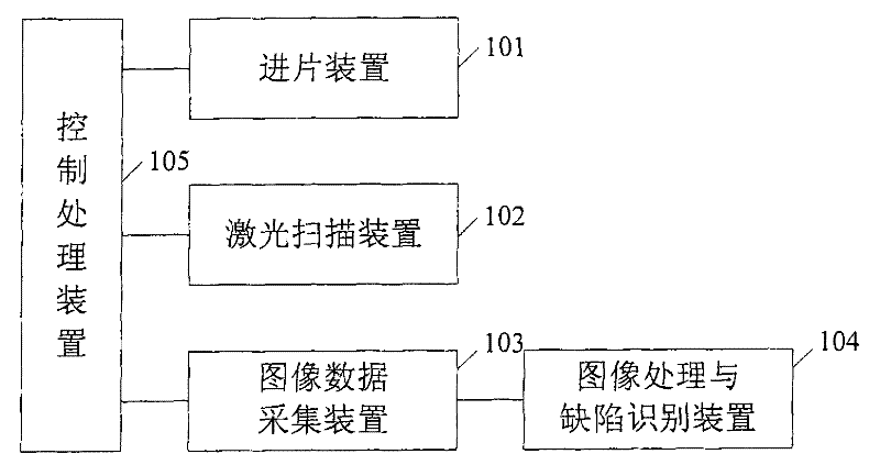
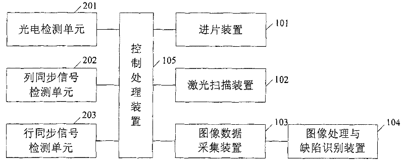
[0015] figure 1 It is a system logic block diagram of the embodiment of the present invention. like figure 1 As shown, the system includes: a film feeding device 101, which includes an inner drum structure for attaching a curved imaging plate, and the film feeding device is used to drive the imaging plate to move along the axis of the inner drum structure; The laser scanning device 102 is used to scan the imaging plate with a laser, and realizes the progressive scanning of the imaging plate along with the movement of the imaging plate; the image data acquisition device 103 is used to collect the imaging plate Excited fluorescent information, converting the fluorescent information into digital information; image processing and defect identification device 104, used to process the digital information to generate weld image information, and per...
PUM
 Abstract
Description
Claims
Application Information