
Method for improving surface performance

A technology of surface performance and surface treatment, applied in metal material coating technology, electrical components, semiconductor/solid-state device manufacturing, etc., can solve problems such as high cost, poor surface performance of wafers, and changes in electrical properties of insulating layers, and achieve low cost , improve surface properties, repair the effect of reducing surface properties

Inactive Publication Date: 2010-07-28
SEMICON MFG INT (SHANGHAI) CORP
View PDF0 Cites 4 Cited by
  • Summary
  • Abstract
  • Description
  • Claims
  • Application Information

AI Technical Summary

Problems solved by technology

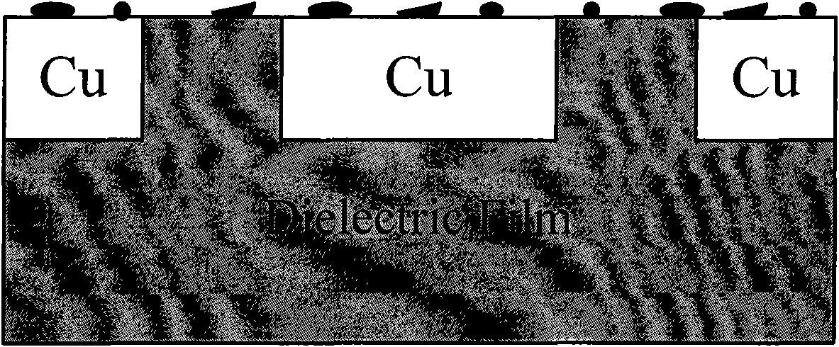
[0014] During the grinding of the connected metal layer by CMP and the simultaneous processing of the insulating layer and the metal layer, due to the simultaneous chemical reaction and mechanical grinding, the Cu atomic bonds on the surface of the metal layer will be separated by chemical reaction and mechanical grinding. Under the action of grinding, it is destroyed to form free Cu ions. These free ions can not only move freely on the surface of the metal layer, but also enter the insulating layer through diffusion migration, resulting in changes in the electrical properties of the insulating layer (that is, its electrical conductivity). enhanced), such as figure 2 As shown, this ion migration will not only reduce the breakdown voltage of the insulating layer between the through holes, but also cause a leakage current (LeakageCurrent) to form in the final circuit structure, seriously reducing the performance of the wafer;
[0015] In addition, during the Q time period, due to the unsatisfactory storage environment of the wafer, the storage environment often contains a considerable amount of organic particles, some of which may settle on the surface of the wafer or be adsorbed to the surface of the wafer by the Cu ions , thereby forming surface impurity pollution; on the other hand, a part of the Cu ions will also combine with oxygen in the preservation environment to slowly oxidize, thereby forming Cu oxides on the wafer surface, such as figure 2 As shown, obviously, the generation of these surface impurities and oxides will further reduce the performance of the wafer
[0016] Since CMP is already a mature and fixed process, if it needs to be improved, it is necessary to modify the CMP equipment on the integrated circuit processing line, which is very expensive; in addition, the wafer storage environment during the Q time period involves too many uncertain factors. If the storage environment of the wafer is improved according to the strict purification storage requirements, not only the cost is too high, but also it is difficult to achieve the desired improvement effect, and the operability is not strong
Therefore, for the problem that the longer the Q time is, the worse the surface performance of the wafer is, the existing technology cannot provide an effective solution

Method used


Image

  • Method for improving surface performance
  • Method for improving surface performance
  • Method for improving surface performance

Examples


Embodiment Construction

[0032] In order to make the object, technical solution and advantages of the present invention clearer, the present invention will be further described in detail below with reference to the accompanying drawings and examples.

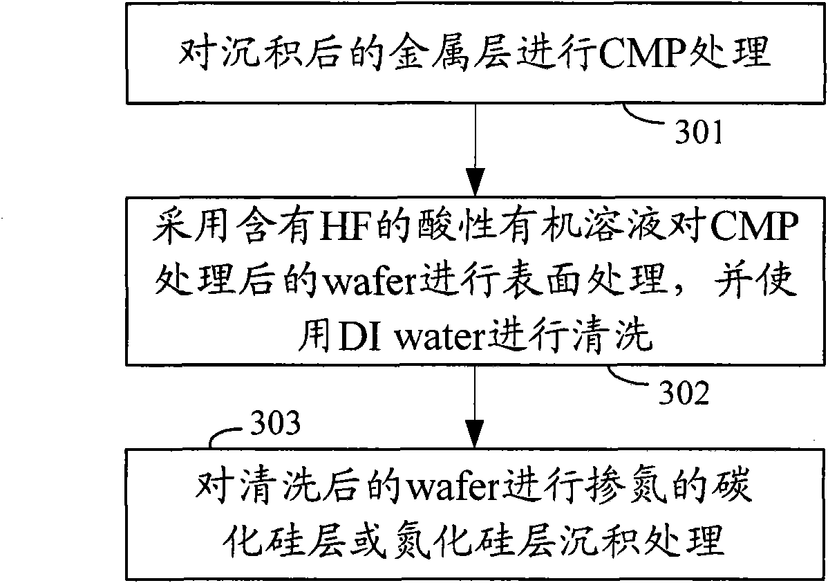
[0033] The core idea of ​​the method for improving surface properties proposed by the present invention is that after the CMP for the metal layer is completed, after the Q time including possible sub-processes, the CVD method is not immediately performed to generate NDC / Si 3 N 4 layer main process, but performing the CVD method to generate NDC / Si 3 N 4 Add a step of cleaning the wafer surface before the main process of the layer. Since the implementation of the sub-process does not affect the realization of the present invention, it will be omitted in the following narration, and only explained from the execution order of the main process, the improved flow process is as follows image 3 shown, including:

[0034] Step 301: performing CMP treatment ...


PUM


Abstract

The invention discloses a method for improving surface performance. After a deposited metal layer is subjected to chemically mechanical polishing and before a silicon carbide layer or a silicon nitride layer for performing nitrogen doping on wafers is deposited, the method further comprises the steps of: performing surface treatment on the wafers after the chemically mechanical polishing by adopting acidic organic solution containing hydrofluoric acid, and washing the wafers by using deionized water. In the method for improving the surface performance, by using the acidic organic solution containing HF, free metal ions on the surfaces of the wafers can be reduced, metallic oxides can be eliminated and organic particles causing surface contamination can be dissolved; the reduction of the surface performance of the wafers during Q time is effectively repaired; and compared with the prior art, the method effectively improves the surface performance of the wafers, and an improved machining process applied cannot cause cost increase.

Description

technical field [0001] The invention relates to integrated circuit processing and manufacturing technology, in particular to a method for improving surface properties. Background technique [0002] In the integrated circuit manufacturing process, the wafer (wafer) processing technology is in the most core and critical position, and the quality of the wafer processing technology has a decisive influence on the working performance of the final gate circuit. [0003] Among them, in the post-processing process of the wafer, after the deposition of the metal layer to the contact hole (Contact Hole) is completed, it is necessary to perform chemical mechanical polishing (CMP) on the deposited metal layer (usually metal copper Cu). ), the wafer section structure before CMP treatment is as follows figure 1 As shown on the left side of the middle, the lower dark area at this time is the insulating layer (Dielectric Film) made of low dielectric constant material (Lowk Material, LkM). ...

Claims


Application Information

Patent Timeline
Patent Type & Authority Applications(China)
IPC IPC(8): H01L21/3213C23C22/06
Inventor 卑多慧
Owner SEMICON MFG INT (SHANGHAI) CORP
Learn More