
Super structure based on vertical gate SOI CMOS device and manufacturing method thereof

A fabrication method and vertical gate technology, applied in semiconductor/solid-state device manufacturing, electrical solid-state devices, semiconductor devices, etc., can solve the problems of reducing source-drain breakdown voltage, reducing device gain, increasing power consumption, etc., and achieving the optimization of electric field distribution , The effect of improving the breakdown voltage

Inactive Publication Date: 2010-07-28
SHANGHAI INST OF MICROSYSTEM & INFORMATION TECH CHINESE ACAD OF SCI +1
View PDF0 Cites 5 Cited by
  • Summary
  • Abstract
  • Description
  • Claims
  • Application Information

AI Technical Summary

Problems solved by technology

The unique floating body effect of SOI CMOS devices will not only reduce device gain, reduce source-drain breakdown voltage, cause single-transistor latch-up, bring large leakage current, increase power consumption, but also cause circuit instability, resulting in Noise overshoot that can have a significant impact on device and circuit performance

Method used


Image

  • Super structure based on vertical gate SOI CMOS device and manufacturing method thereof
  • Super structure based on vertical gate SOI CMOS device and manufacturing method thereof
  • Super structure based on vertical gate SOI CMOS device and manufacturing method thereof

Examples


Embodiment 1

[0050] This embodiment provides a super junction structure based on a vertical gate SOI CMOS device, including an SOI substrate, and a gate region, a source region, a channel region, and a drain region grown on the SOI substrate, and the channel region and the drain region A drift region with pn column regions arranged up and down is arranged between the regions, and the doping type of the lower column region in the drift region is consistent with that of the drain region.

[0051] The SOI substrate includes a silicon substrate layer grown from bottom to top, a buried oxide layer, and a single crystal silicon top layer. The super junction structure of the vertical gate SOI CMOS device includes a vertical gate SOI NMOS super junction structure and a vertical gate SOIPMOS super junction structure, the gate area is divided into an NMOS gate area and a PMOS gate area, and the source area is divided into an NMOS source area and a PMOS source area region, the channel region is divid...

Embodiment 2

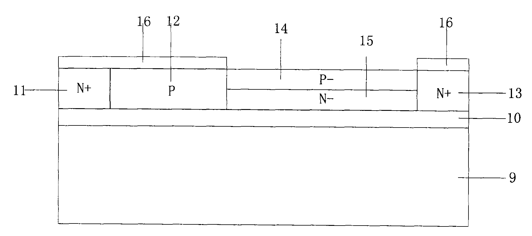
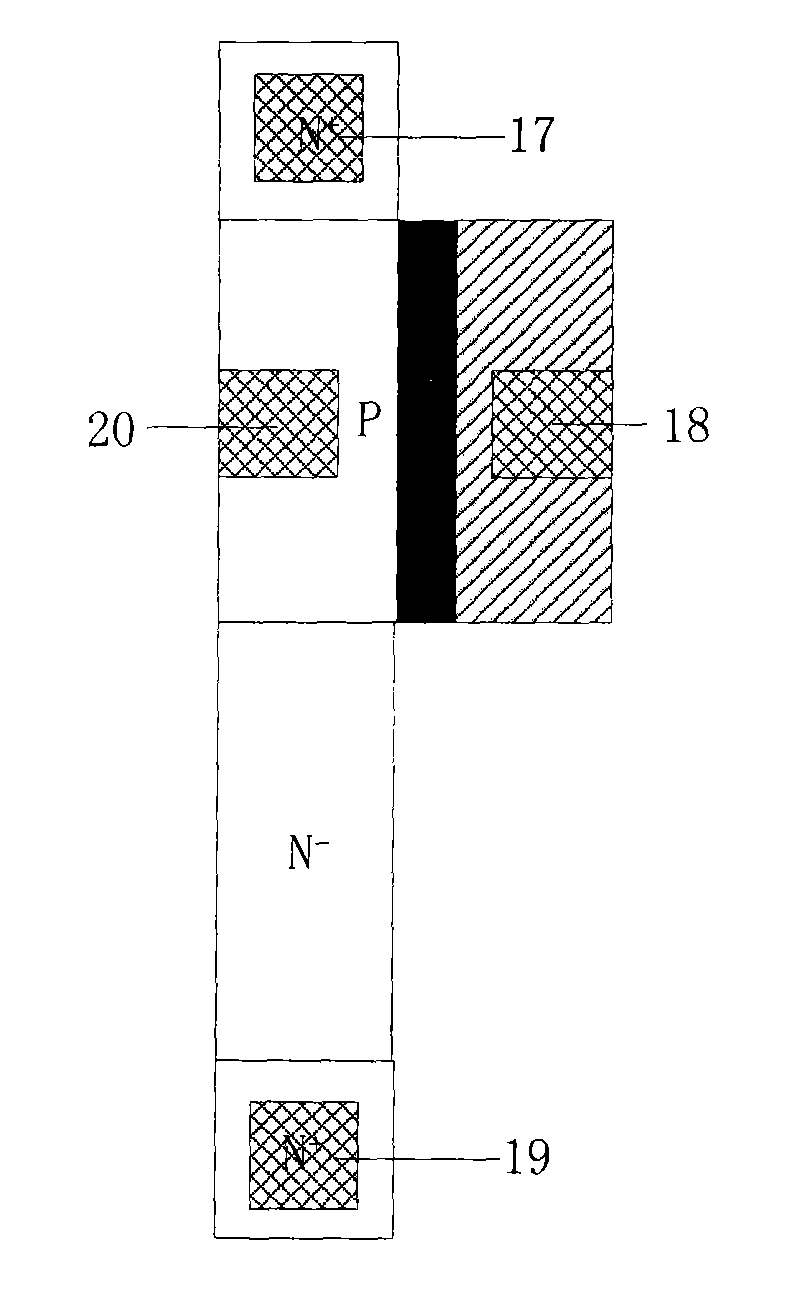
[0067] Such as figure 2 , 3 As shown, this embodiment provides a super junction structure based on a vertical gate SOI NMOS device, including an SOI substrate, and an NMOS source region 11, an NMOS channel region 12, and an NMOS drain region 13 grown on the SOI substrate. Between the NMOS channel region 12 and the NMOS drain region 13 there is a drift region with pn junctions arranged up and down, and the doping type of the junction region below is consistent with that of the NMOS drain region 13 . In the NMOS super junction structure, the upper junction region is the n-pillar region 14 , and the lower junction region is the p-pillar region 15 .

[0068] The SOI substrate includes a silicon substrate layer 9 grown from bottom to top, a buried oxide layer 10, and a single crystal silicon top layer. An NMOS vertical gate region is grown on one side of the NMOS channel region 12 , and an NMOS gate oxide layer is grown between the NMOS vertical gate region and the NMOS channel ...

Embodiment 3

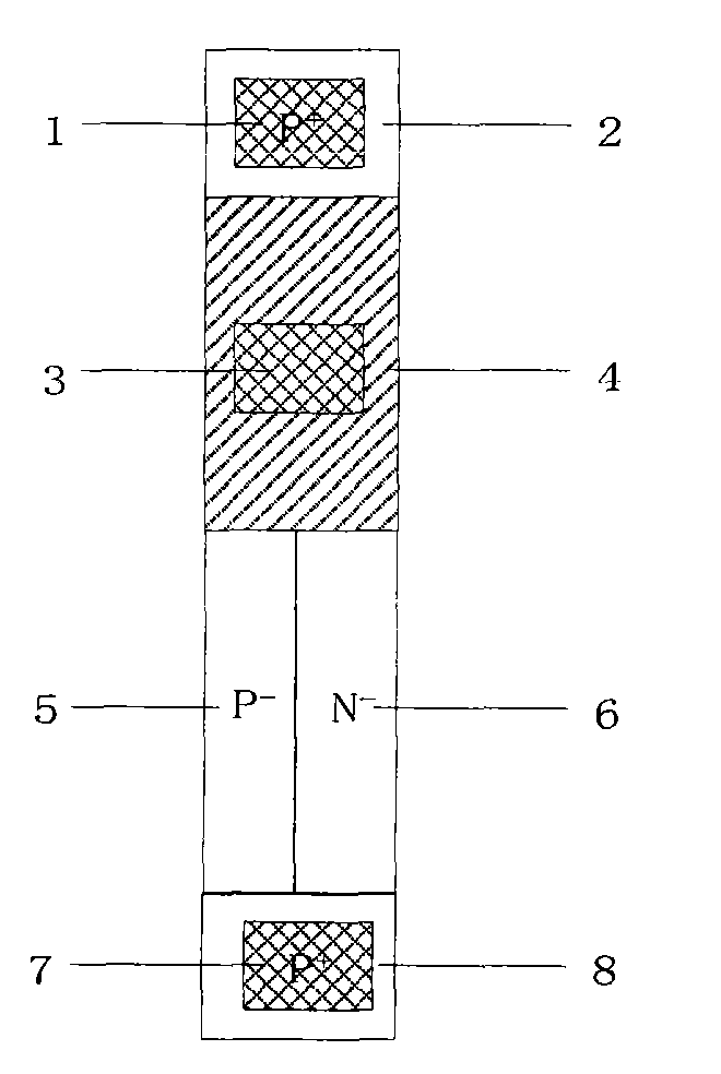
[0071] Such as Figure 4 , 5 As shown, this embodiment provides a super junction structure based on a vertical gate SOI PMOS device, including an SOI substrate, and a PMOS source region 21, a PMOS channel region 22, and a PMOS drain region 23 grown on the SOI substrate. Between the PMOS channel region 22 and the PMOS drain region 23 there is a drift region with pn junctions arranged up and down, and the doping type of the junction region below is consistent with that of the PMOS drain region 23 . In the PMOS superjunction structure, the upper junction region of the drift region is the p-pillar region 24 , and the lower junction region is the n-pillar region 25 .

[0072] The SOI substrate includes a silicon substrate layer 9 grown from bottom to top, a buried oxide layer 10, and a single crystal silicon top layer. A PMOS vertical gate region is grown on one side of the PMOS channel region 22 , and a PMOS gate oxide layer is grown between the PMOS vertical gate region and the...


PUM


Abstract

The invention discloses a super structure based on a vertical gate SOI CMOS device and a manufacturing method thereof. The structure comprises an SOI substrate, a gate region, a source region, a channel region, a drift region and a drain region, wherein the gate region, the source region, the channel region, the drift region and the drain region grow on the SOI substrate; the gate region is vertical to and in direct contact with a buried oxide layer; the drift region in which pn column regions are arranged up and down is arranged between the channel region and the drain region; and the doping type of the lower column region in the drift region is consistent with the doping type of the drain region. On the basis of the vertical gate SOI CMOS device, the invention transforms the single doping type drift region into the drift region in which the pn column regions are arranged alternately, enables the drift region to be fully exhausted as much as possible when the breakdown voltage is achieved, optimizes the distribution of each electric field, reduces and levels the peak values of electric fields at the drift region, the junction of the drift region and the channel region and the junction of the drift region and the drain region, keeps the function of the vertical gate SOI CMOS device for eliminating the floating-body effect, and simultaneously greatly improves the high-voltage breakdown resistance of the SOI LDMOS.

Description

technical field [0001] The invention belongs to the technical field of microelectronics and solid electronics, and relates to a superjunction structure based on a vertical gate SOI CMOS device and a manufacturing method thereof. Background technique [0002] SOI (Silicon-On-Insulator) integration technology is known as the integration technology of the 21st century due to its advantages of good isolation performance, small leakage current, fast speed, low power consumption and radiation resistance, and is widely used in high-end Performance HVIC and PIC. [0003] However, due to the dielectric isolation of SOI materials, Si-SiO 2 The depletion layer at the interface is not in contact, and there is a neutral body region between them. This neutral body region makes the silicon body in an electrically floating state, resulting in two obvious secondary parasitic effects, one is "warping Effect", that is, the Kink effect; the other is the base open-circuit NPN parasitic transis...

Claims


Application Information

Patent Timeline
Patent Type & Authority Applications(China)
IPC IPC(8): H01L27/12H01L29/78H01L29/38H01L21/84
Inventor 程新红何大伟俞跃辉肖德元王中健徐大朋
Owner SHANGHAI INST OF MICROSYSTEM & INFORMATION TECH CHINESE ACAD OF SCI
Learn More