Confocal optical scanner

A scanner and confocal technology, which is applied in the field of biomedical microscopy imaging, can solve the problems of uneven illumination intensity, high stray light background noise, and slow scanning speed of the turntable confocal scanner, and achieve high-sensitivity confocal optical imaging , avoid stray light background noise, avoid the effect of scanning fringe interference

Inactive Publication Date: 2010-08-04
赖博
View PDF7 Cites 17 Cited by
  • Summary
  • Abstract
  • Description
  • Claims
  • Application Information

AI Technical Summary

Problems solved by technology

[0007] The purpose of the present invention is to improve the deficiencies of various current confocal optical scanners, such as the slow scanning speed and low sensitivity of single-point confocal laser scanners, and the high stray light background noise of rotary disk confocal scanners , bright and dark fringe interference, uneven illumination intensity, etc., a new confocal optical scanner is provided to obtain high-quality confocal images at high speed

Method used


Image

  • Confocal optical scanner
  • Confocal optical scanner
  • Confocal optical scanner

Examples


Embodiment 1

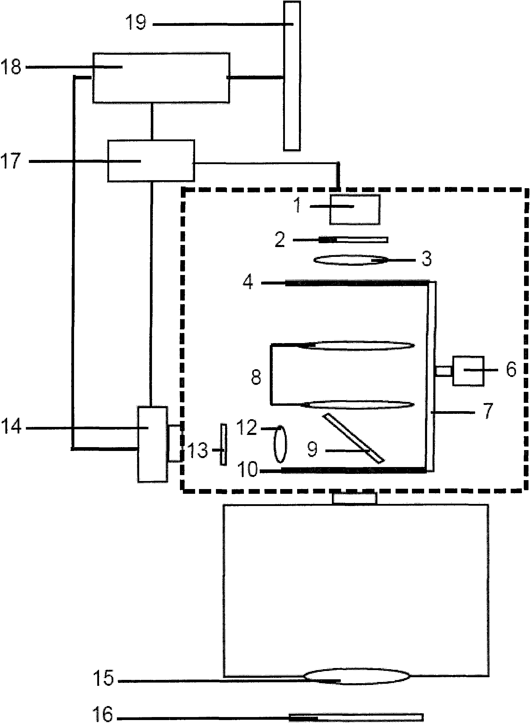
[0044] figure 2 It is a structural schematic diagram of the first confocal optical scanner related to the present invention, Figure 6 It is a structural schematic diagram of the illumination slider 4 and the imaging slider 10 used in this embodiment.

[0045] In this embodiment, the illuminating light emitted by the light source 1 composed of mercury lamp, xenon lamp, light emitting diode or laser passes through the pinhole 5 on the illuminating color filter 2, illuminating lens 3, and illuminating slider 4 which are sequentially placed in the optical path. , the pinhole lens group 8, the dichroic beam splitter 9, the pinhole 11 and the microscope objective lens 15 on the imaging slider 10, shine on the sample 16 of the imaging focal plane of the microscope objective lens 15, wherein only the illumination light of a specific wavelength can pass through Lighting filter 2. Fluorescence emitted by the illuminated sample 16 returns through the microscope objective lens 15 and ...

Embodiment 2

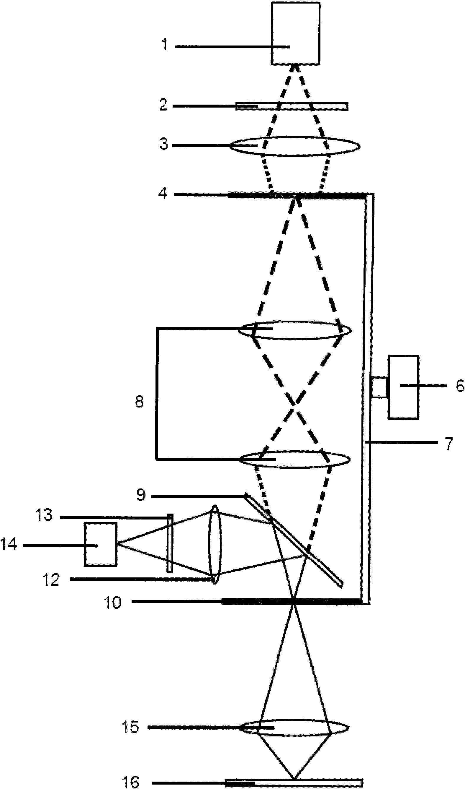
[0050] image 3 It is a schematic diagram of the structure of the second confocal optical scanner related to the present invention. The structure and scanning mode of the illumination slider 4 and the imaging slider 10 are the same as those in Embodiment 1, and the specific differences are as follows:

[0051] The dichroic beam splitter 9 is moved from the middle of the pinhole lens group 8 and the imaging slider 10 to the middle of the pinhole lens group 8, and the distance between the pinhole lens group 8 and the imaging slider 10 is shortened. Therefore, the pinhole lens group 8 can use a lens with a short focal length and a large numerical aperture.

Embodiment 3

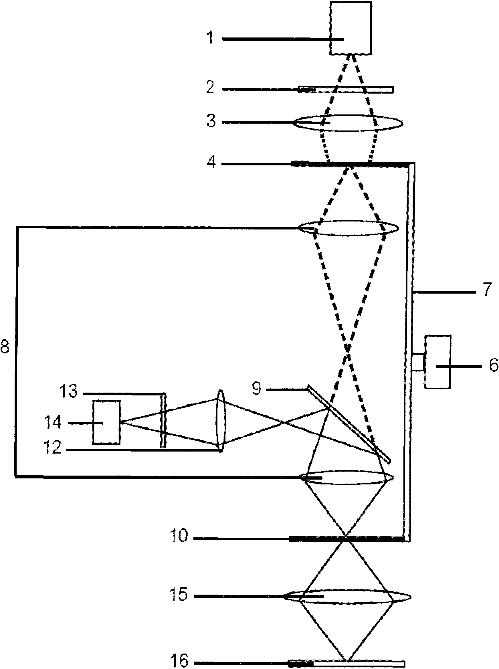
[0053] Figure 4 It is a schematic diagram of the structure of the third confocal optical scanner related to the present invention. The structures and scanning methods of the illumination slider 4 and the imaging slider 10 are the same as those in Embodiment 1, and the specific differences are as follows:

[0054] The illumination slider 4 and the imaging slider 10 are not on the same straight line, but are respectively located on two straight lines perpendicular to each other; the dichroic beam splitter 9 is the most commonly used common dichroic beam splitter, which can pass through the illumination filter The illumination light of 2 reflects the fluorescent light emitted by the sample 16 . After the illumination emitted by the light source 1 sequentially illuminates the color filter 2, the illumination lens 3, the pinhole 5 on the illumination slider 4, and the pinhole lens group 8, it is reflected by the dichroic beam splitter 9 and passes through the holes on the imaging ...


PUM


Abstract

The invention relates to a confocal optical scanner, in particular to a multiple-pinhole confocal optical scanner. The confocal optical scanner is mainly characterized in that an opaque illuminating sliding block and an opaque imaging sliding block, on which a plurality of nonopaque pinholes are arrayed, are driven to slide in a reciprocating way at set constant speed so as to scan a sample, the pinholes on the illuminating sliding block coincide with the pinholes on the illuminating sliding block on by one in the projective center formed on the sample through a pinhole lens group and an objective lens of a microscope, the pinholes are regularly arrayed on the illuminating sliding block and the opaque imaging sliding block, any two adjacent rows of pinholes keep the equal row distance, and any two columns of pinholes keep the equal column distance. Because the illuminating sliding block and the opaque imaging sliding block, on which a plurality of nonopaque pinholes are arrayed, are driven to slide in a reciprocating way at set constant speed so as to scan the sample, the confocal optical scanner has high speed, zero stray light background noise and uniform illumination intensity and can be easily synchronized with the camera exposure control.

Description

technical field [0001] The invention relates to a confocal optical scanner, in particular to a multi-pinhole confocal scanner using area array detectors such as a charge coupled device (CCD) and a complementary metal oxide semiconductor (Complementary Metal Oxide Semiconductor, CMOS) as a detector. Focus the optical scanner. The invention is mainly used in the field of biomedical microscopic imaging, and can also be used in material research and integrated circuit chip detection imaging. Background technique [0002] With the deepening of cell biology research, the application of microscopy imaging has become more and more common, and fluorescence microscopy imaging has received extensive attention, especially live cell fluorescence real-time imaging. However, ordinary wide-field fluorescence microscopes have the problem of low axial resolution, especially when observing some thicker samples, which even limits the use of fluorescence microscopes. In order to solve the prob...

Claims


Application Information

Patent Timeline
Patent Type & Authority Applications(China)
IPC IPC(8): H04N1/04G01N21/01G01N21/64
Inventor 赖博
Owner 赖博
Why Eureka
Try Eureka