Method for regulating metallic silicides source/drain Schottky barrier height

A technology of metal silicide source and Schottky potential, which is applied in semiconductor/solid-state device manufacturing, electrical components, circuits, etc., can solve the problems of reduced driving current and increased leakage current, and achieves reduced difficulty and cost and continuous regulation Ability, easy to adjust the effect

Inactive Publication Date: 2010-08-18
INST OF MICROELECTRONICS CHINESE ACAD OF SCI
View PDF0 Cites 22 Cited by
  • Summary
  • Abstract
  • Description
  • Claims
  • Application Information

AI Technical Summary

Problems solved by technology

[0003] However, the Schottky MOSFET (SB MOSFET) in the on state, due to the larger Schottky barrier height (SBH) of the source / channel, the drive current is reduced; while in the off state, due to the smaller drain / channel SBH, making the leakage current increase

Method used


Image

  • Method for regulating metallic silicides source/drain Schottky barrier height
  • Method for regulating metallic silicides source/drain Schottky barrier height
  • Method for regulating metallic silicides source/drain Schottky barrier height

Examples


Embodiment Construction

[0028] In order to make the object, technical solution and advantages of the present invention clearer, the present invention will be described in further detail below in conjunction with specific embodiments and with reference to the accompanying drawings.

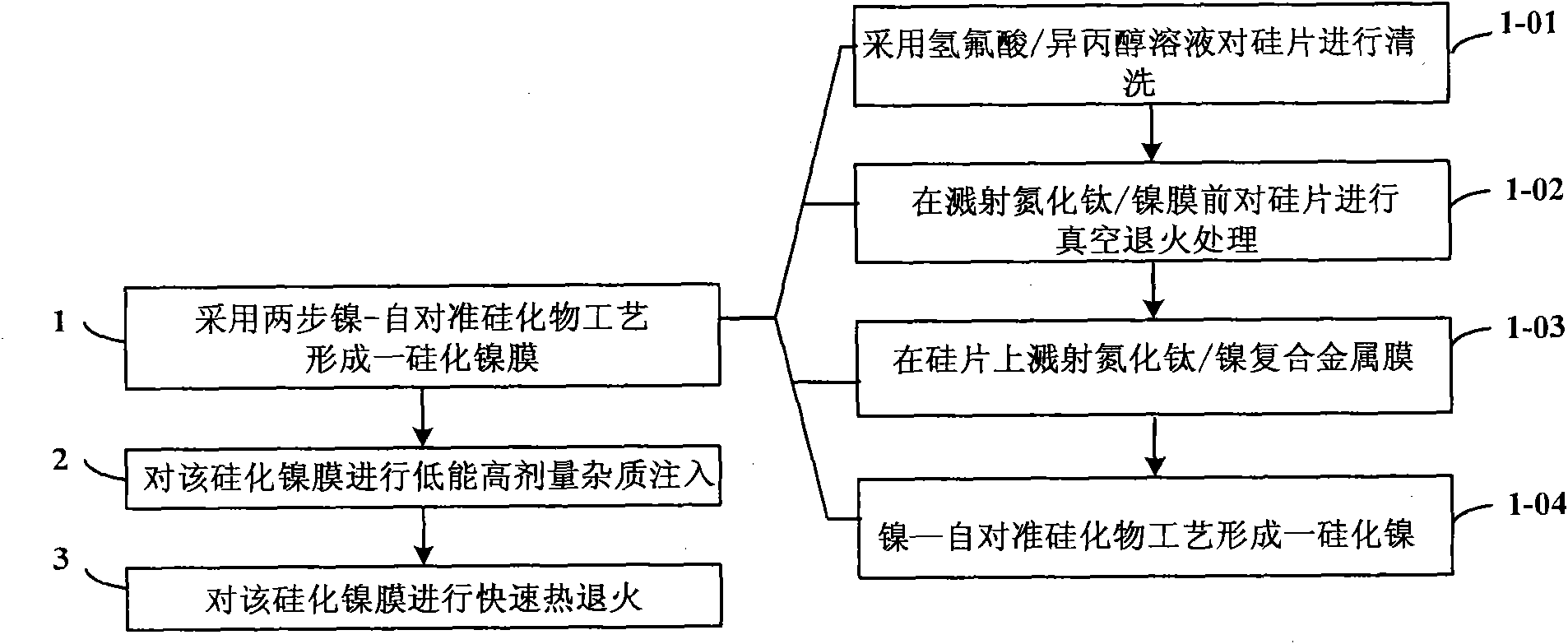
[0029] Such as figure 1 as shown, figure 1 It is a flow chart of a method for adjusting the height of metal silicide source / drain Schottky barriers provided by the present invention, and the method includes:

[0030] Step 1: Form a nickel silicide film using a two-step nickel-salicide process; specifically include:

[0031] First, the silicon chip is cleaned with hydrofluoric acid / isopropanol solution; that is, after routine cleaning, it is cleaned in hydrofluoric acid / isopropanol solution, and the proportion (volume ratio) of hydrofluoric acid / isopropanol solution is : hydrofluoric acid: isopropanol: deionized water=37.5ml: 6ml: 3000ml, soaked for 40 seconds at room temperature;

[0032] Then, vacuum anneal the silico...


PUM


Abstract

The invention discloses a method for regulating metallic silicides source / drain Schottky barrier height. The method comprises the steps as follows: step 1: using a two-step nickel-self-alignment silicide process to form a nickel silicide film; step 2: injecting low energy high dosage impurities to the nickel silicide film; and step 3: rapidly thermally annealing the nickel silicide film. The invention has the advantages of capability of using the existing process, simple process, easy operation, low cost and easy integration, thereby achieving good compatibility with CMOS process.

Description

technical field [0001] The invention relates to the field of microelectronic ultra-deep submicron technology complementary metal oxide semiconductor device (CMOS) and ultra-large-scale integration technology, in particular to a method for adjusting the height of a metal silicide source / drain Schottky barrier. Background technique [0002] When the gate length of MOSFET devices is reduced to the nanometer scale, the metal source / drain (S / D) structure has a series of advantages: the atomic-level abrupt junction can suppress the short channel effect (SCE), low S / D series resistance and contact Resistance, the low-temperature process of S / D formation is suitable for integrating new materials such as high-k gate dielectric, metal gate and strained silicon, making it the most promising substitute for doped silicon S / D structure. [0003] However, the Schottky MOSFET (SB MOSFET) in the on state, due to the larger Schottky barrier height (SBH) of the source / channel, the drive curren...

Claims


Application Information

Patent Timeline
Patent Type & Authority Applications(China)
IPC IPC(8): H01L21/336
Inventor 尚海平徐秋霞
Owner INST OF MICROELECTRONICS CHINESE ACAD OF SCI
Why Eureka
Try Eureka