

Crystallization temperature-adjustable Ga30Sb70/Sb80Te20 nano composite multi-layer phase-change thin-film material
A sb80te20, nanocomposite technology, applied in the field of microelectronics, can solve the problems of unfavorable crystallization temperature to thermal stability of memory devices, slow crystallization speed, affecting the programming speed of phase change memory, etc., to reduce programming power consumption, fast crystallization speed, good The effect of thermal stability
- Summary
- Abstract
- Description
- Claims
- Application Information
AI Technical Summary
Problems solved by technology
Method used
Image

Examples
Embodiment 1
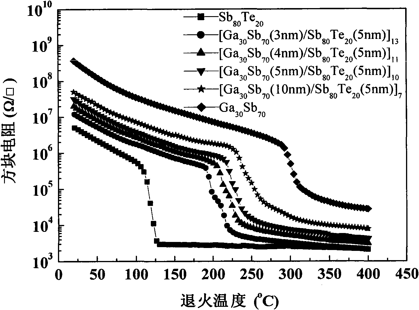
[0031] Ga prepared in this example 30 Sb 70 / Sb 80 Te 20 The nanocomposite multilayer phase change film material structure is specifically [Ga 30 Sb 70 (3nm) / Sb 80 Te 20 (5nm)] 13 , [Ga 30 Sb 70 (4nm) / Sb 80 Te 20 (5nm)] 11 , [Ga 30 Sb 70 (5nm) / Sb 80 Te 20 (5nm)] 10 and [Ga 30 Sb 70 (10nm) / Sb 80 Te 20 (5nm)] 7 , and the Ga 30 Sb 70 / Sb 80 Te 20 The total thickness of the nanocomposite multilayer phase change film material is 100nm.
[0032] The preparation steps are:
[0033] 1) Clean SiO2 2 / Si(100) substrate: clean the surface and back, remove dust particles, organic and inorganic impurities; strong ultrasonic cleaning in acetone solution for 3-5 minutes, rinse with deionized water; then strong ultrasonic cleaning in ethanol solution for 3-5 minutes, rinse with deionized water, high-purity N 2 Dry the surface and back; dry the water vapor in an oven at 120°C for about 20 minutes;
[0034] 2) Prepare the alloy target: set the radio frequency power...
Embodiment 2
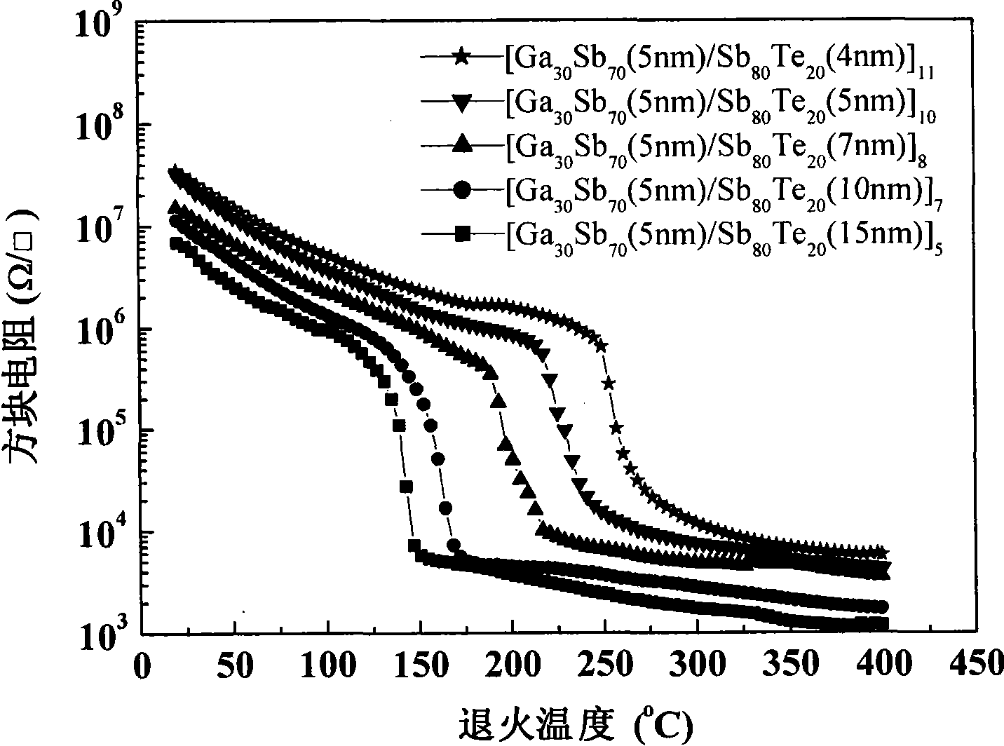
[0037] Ga prepared in this example 30 Sb 70 / Sb 80 Te 20 The nanocomposite multilayer phase change film material structure is specifically [Ga 30 Sb 70 (5nm) / Sb 80 Te 20 (15nm)] 5 , [Ga 30 Sb 70 (5nm) / Sb 80 Te 20 (10nm)] 7 , [Ga 30 Sb 70 (5nm) / Sb 80 Te 20 (7nm)] 8 , [Ga 30 Sb 70 (5nm) / Sb 80 Te 20 (5nm)] 10 and [Ga 30 Sb 70 (5nm) / Sb 80 Te 20 (4nm)] 11 , and the Ga 30Sb 70 / Sb 80 Te 20 The total thickness of the nanocomposite multilayer phase change film material is 100nm.
[0038] The preparation steps are:
[0039] 1) Clean SiO2 2 / Si(100) substrate: clean the surface and back, remove dust particles, organic and inorganic impurities; strong ultrasonic cleaning in acetone solution for 3-5 minutes, rinse with deionized water; then strong ultrasonic cleaning in ethanol solution for 3-5 minutes, rinse with deionized water, high-purity N 2 Dry the surface and back; dry the water vapor in an oven at 120°C for about 20 minutes;
[0040] 2) Prepare t...
PUM
| Property | Measurement | Unit |
|---|---|---|
| thickness | aaaaa | aaaaa |
| thickness | aaaaa | aaaaa |
| crystallization temperature | aaaaa | aaaaa |
Abstract
Description
Claims
Application Information