Method and device for growing silicon carbide signal crystals based on physical vapor transport technology
A technology of physical vapor transport and silicon carbide, applied in chemical instruments and methods, single crystal growth, single crystal growth, etc., can solve problems such as large crystal stress, crystal growth failure, polycrystalline rings, etc.
Active Publication Date: 2010-08-25
安徽微芯长江半导体材料有限公司
View PDF5 Cites 19 Cited by
- Summary
- Abstract
- Description
- Claims
- Application Information
AI Technical Summary
Problems solved by technology
If organic or inorganic substances are used to paste the seed crystal to the top of the crucible, due to the inconsistent thermal expansion coefficients of the seed crystal and the crucible, it is easy to cause the seed crystal to fall off during the crystal growth process, especially during the heating process, resulting in crystal growth failure; A support made of graphite or metal fixes the seed crystal to the top of the crucible, so the seed crystal will not fall off during the crystal growth process, but because the surrounding of the seed crystal is covered by graphite or metal support, polycrystalline rings appear around the growing crystal
At the same time, regardless of the method of pasting the seed crystal or the method of fixing the seed crystal with a bracket, stress will inevitably be applied to the inside of the seed crystal, resulting in greater internal stress in the grown crystal.
Method used
View moreImage
Smart ImageViewing Examples
Examples
Embodiment 1
Embodiment 2
Login to View More PUM
| Property | Measurement | Unit |
|---|---|---|
| thickness | aaaaa | aaaaa |
| height | aaaaa | aaaaa |
| diameter | aaaaa | aaaaa |
Abstract
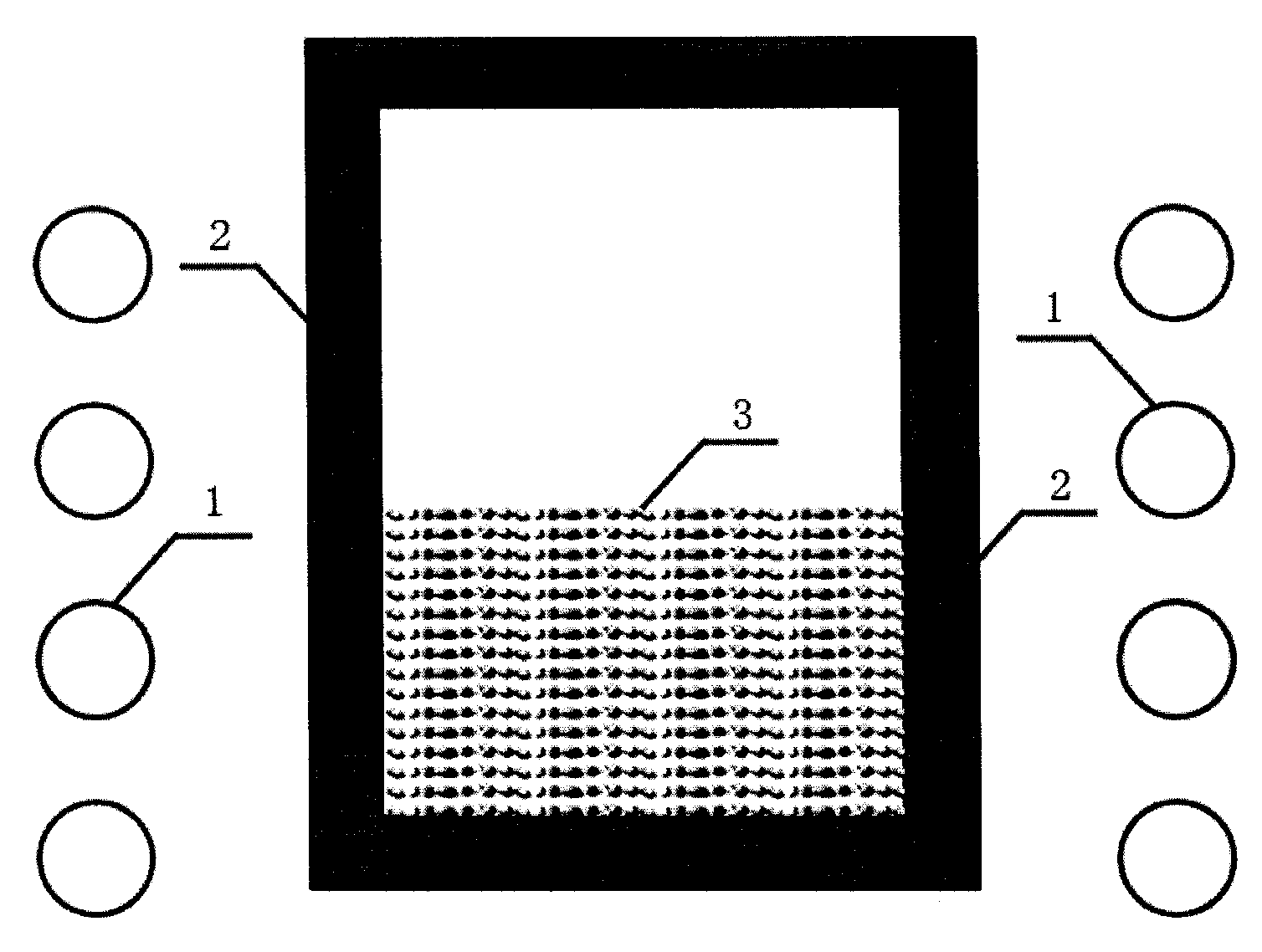
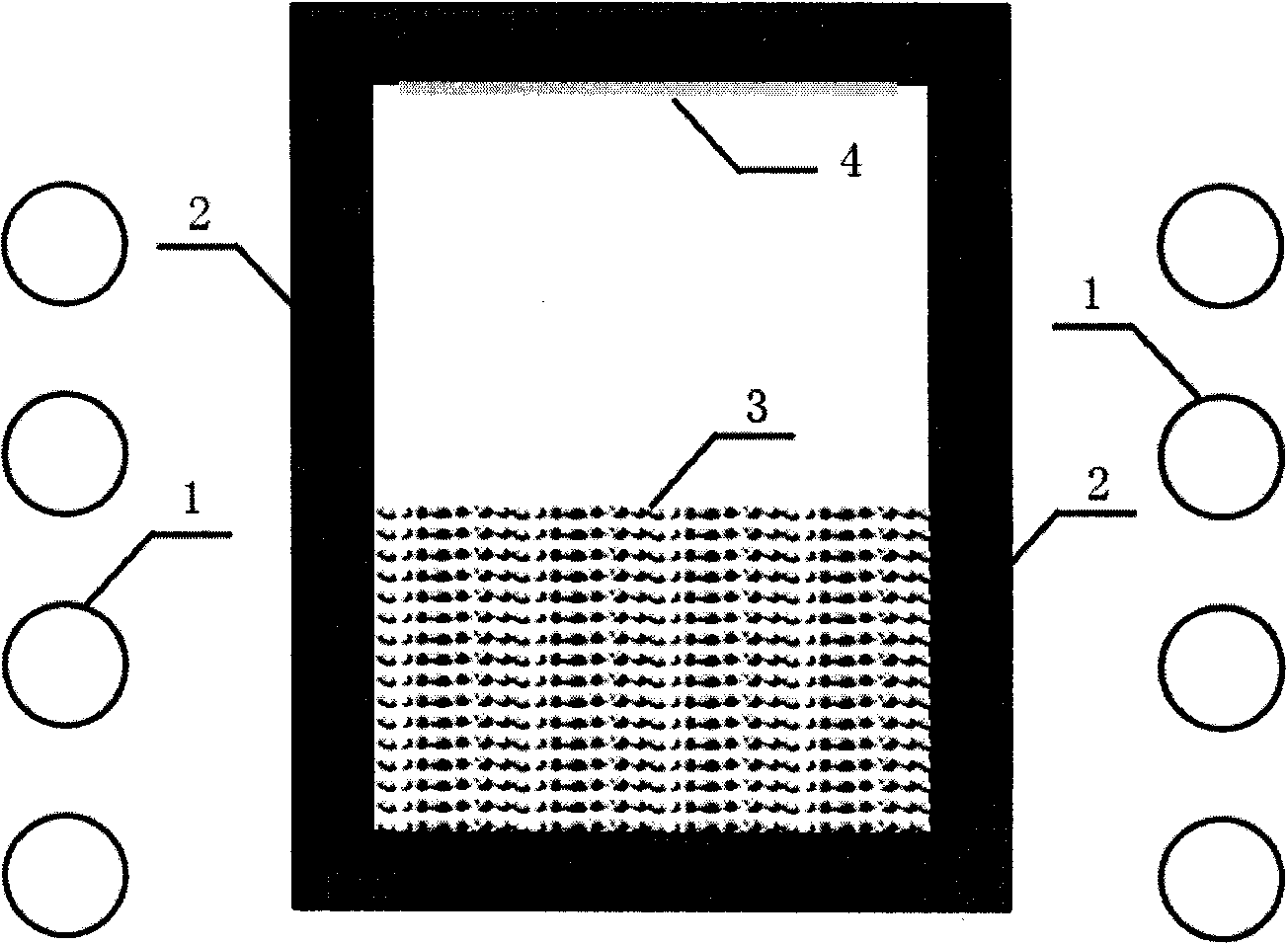
The invention belongs to the technical field of crystal growth and in particular relates to a method and device for growing silicon carbide signal crystals based on physical vapor transport technology. The method is characterized in that seed crystals are positioned at the bottom of a crucible and in the low temperature zone; the raw materials are positioned at the top of the crucible and in the high temperature zone; and in the growth process, the seed crystals are placed at the bottom of the crucible, without being stuck to or fixed on the crucible cover. The method is characterized by using the silicon carbide polycrystalline ingots as the raw materials and fixing the silicon carbide polycrystalline ingots at the top of the crucible. The method and the device can effectively avoid that the crystals obtained during seed crystal shedding or growing in the growth process have excessive stress due to improper seed crystal sticking or fixing, meanwhile, as the polycrystalline ingots are used as the raw materials, the gas phase components are distributed more uniformly in the growth cavity, and the grown crystals have better uniformity and higher growth repeatability.
Description
technical field The invention belongs to the technical field of crystal growth, and in particular relates to a method and a device for growing a silicon carbide single crystal based on a physical vapor transport technology. Background technique Silicon carbide (SiC) is a compound semiconductor with many excellent properties, such as: very high thermal conductivity (about 5.0W / cm, higher than any known metal), so it is very suitable for making Electronic devices operating at high temperatures; high saturation electron mobility (about 2.7x107cm / s) and high breakdown electric field (about 3MV / cm), making it very suitable for making high-voltage, high-frequency devices. At the same time, the Si-C bonding energy is large, which makes SiC very strong in chemical stability and radiation resistance. SiC has become a recognized new-generation semiconductor material that can replace the first-generation semiconductor Si and the second-generation semiconductor GaAs. In addition, hexa...
Claims
Login to View More Application Information
Patent Timeline
 Patent Type & Authority Applications(China)
IPC IPC(8): C30B23/00C30B29/36
Inventor 陈博源陈之战施尔畏严成锋肖兵
Owner 安徽微芯长江半导体材料有限公司


