
Processing method of fuse wire on copper interconnection layer and semiconductor device thereof

A technology of copper interconnection and manufacturing method, which is applied in the direction of semiconductor devices, semiconductor/solid-state device manufacturing, semiconductor/solid-state device components, etc., can solve the problems of increasing the relative dielectric constant of IMD, complicated operation process, and increased power consumption. Achieve the effects of optimizing electrical performance and operating speed, simplifying process production, and improving parameter matching

Active Publication Date: 2012-05-30
SEMICON MFG INT (SHANGHAI) CORP
View PDF0 Cites 0 Cited by
  • Summary
  • Abstract
  • Description
  • Claims
  • Application Information

AI Technical Summary

Problems solved by technology

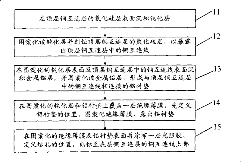
[0016] It can be seen that in steps 2D and 2E of the prior art, two steps of coating photoresist are required to first expose the aluminum liner 102 and then define the fusion hole 104. If only one photoresist coating is performed, at the same time define The position of the aluminum liner and the melting hole, the etching passivation layer to expose the aluminum liner and the formation of the melting hole will be carried out at the same time, because the etching depth of the etching passivation layer to expose the aluminum liner and the depth of etching to form the melting hole are Different, so it cannot be realized by one-time photoresist coating, and the operation process is more complicated to realize
[0017] In this copper interconnect process, the etch-stop silicon nitride film has a relative permittivity of about 7, significantly greater than that of silicon oxide of about 4, which increases the relative permittivity of the entire IMD , so that the parasitic capacitance between the copper interconnect lines increases, thus causing the defect of signal delay or increased power consumption

Method used


Image

  • Processing method of fuse wire on copper interconnection layer and semiconductor device thereof
  • Processing method of fuse wire on copper interconnection layer and semiconductor device thereof
  • Processing method of fuse wire on copper interconnection layer and semiconductor device thereof

Examples


Embodiment Construction

[0058] In order to make the object, technical solution, and advantages of the present invention clearer, the present invention will be further described in detail below with reference to the accompanying drawings and examples.

[0059] The present invention has been described in detail using schematic diagrams. When describing the embodiments of the present invention in detail, for the convenience of explanation, the schematic diagram showing the structure will not be partially enlarged according to the general scale, which should not be used as a limitation of the present invention. In addition, in actual production In , the three-dimensional space dimensions of length, width and depth should be included.

[0060] The manufacturing method of the fuse on the copper interconnection layer in the present invention comprises the following steps:

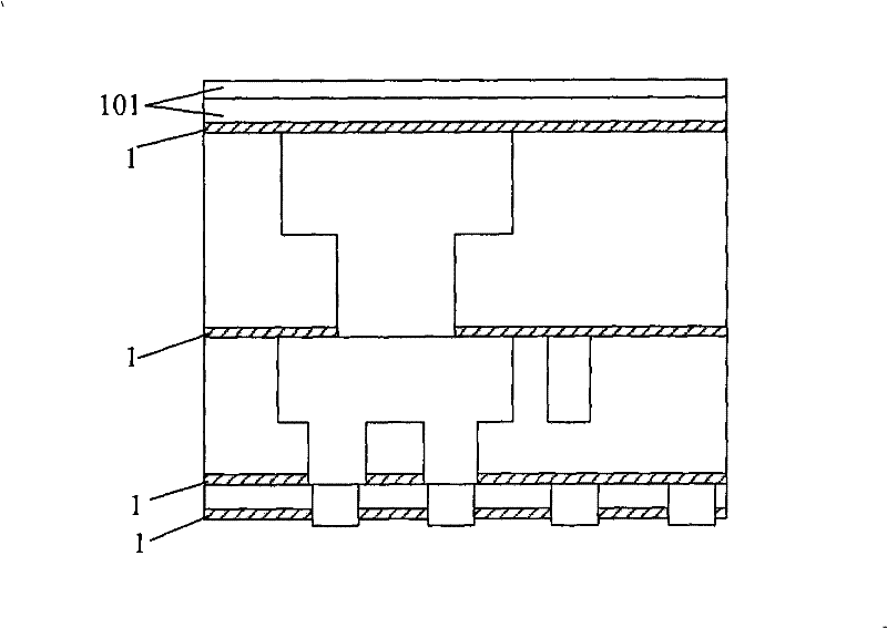
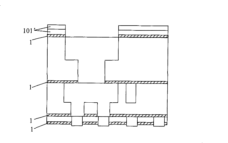
[0061] Step 31, first depositing a passivation layer on the surface of the silicon nitride layer of the top copper interconnection laye...


PUM

PropertyMeasurementUnit
thicknessaaaaaaaaaa
thicknessaaaaaaaaaa
widthaaaaaaaaaa

Abstract

The invention discloses a processing method of a fuse wire on a copper interconnection layer and a semiconductor device thereof. The copper interconnection layer comprises a top copper interconnection layer, a middle copper interconnection layer and a bottom copper interconnection layer. The invention is characterized in that the method comprises the following steps: depositing a passivation layer on the top copper interconnection layer; patterning the passivation layer, and etching until a copper interconnection line in the top copper interconnection layer is exposed; depositing a metallic aluminum layer on the surface of the patterning passivation layer and the surface of the interconnection line of the top copper interconnection layer; pattering the metallic aluminum layer, and formingan aluminum gasket connected with the interconnection line of the top copper interconnection layer; defining the position of a fused hole on the patterning passivation layer, and etching to form the fused hole; depositing a polyimide film on the surface of the aluminum gasket, the surface of the patterning passivation layer and the bottom surface of the fused hole; and removing the polyimide filmon the surface of the aluminum gasket and on the bottom surface of the crater. The invention also discloses a semiconductor device. The method can simplify the technical manufacture procedure, and the semiconductor device can improve the electrical property and the operation speed of the device.

Description

technical field [0001] The invention relates to the technical field of semiconductor manufacturing, in particular to a manufacturing method of a fuse on a copper interconnection layer and a semiconductor device thereof. Background technique [0002] Along with the miniaturization and high integration of semiconductor devices, downscaling of internal interconnections and realization of multilayer internal interconnections have begun. In the interconnection process, a trench for interconnection patterns is formed in the intermetal dielectric layer (Intermetal Dielectric, IMD), and the interior of the trench is buried with interconnection materials, and then the interconnection material outside the trench is removed, only The interconnect material is left inside the trench. In this way, interconnect lines are formed which are buried in the IMD. Copper is increasingly used as an interconnect material because copper can achieve lower resistance than aluminum. Copper interconne...

Claims


Application Information

Patent Timeline
Patent Type & Authority Patents(China)
IPC IPC(8): H01L21/768H01L21/312H01L21/027H01L23/522H01L23/525
Inventor 魏秉钧陈昱升
Owner SEMICON MFG INT (SHANGHAI) CORP
Learn More