Manufacturing method of thin film transistor and transistor manufactured by method

A technology of thin film transistors and manufacturing methods, applied in the direction of transistors, semiconductor/solid-state device manufacturing, electrical components, etc., can solve the problems of complex process, complex production process of thin film transistors, high production cost, etc., and achieve small electrode area, large numerical aperture, The effect of simplifying the manufacturing process

Active Publication Date: 2010-09-22
SHENZHEN DANBANG INVESTMENT GROUP
View PDF0 Cites 38 Cited by
  • Summary
  • Abstract
  • Description
  • Claims
  • Application Information

AI Technical Summary

Problems solved by technology

This method can also solve the symmetry of the lightly doped drain region, but the process is complicated and still requires two ion implantations
[0008] Existing technologies for manufacturing thin-film transistors with lightly doped drains require high-dose implantation to form the source-drain and low-dose implantation to form the lightly-doped drain. Two ion implantations complicate the production process of thin-film transistors , production costs are too high

Method used


Image

  • Manufacturing method of thin film transistor and transistor manufactured by method
  • Manufacturing method of thin film transistor and transistor manufactured by method
  • Manufacturing method of thin film transistor and transistor manufactured by method

Examples


Embodiment 1

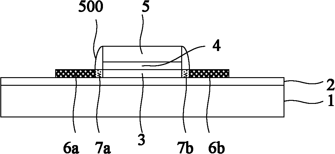
[0028] refer to Figure 4A to Figure 4D , the manufacturing method of the thin film transistor of this embodiment includes the following steps:

[0029] (1) Reference Figure 4A , continuously deposit the surface covering layer 2 and the intrinsic a-Si layer (the intrinsic a-Si layer is the original state of the polysilicon island active layer 300 by PECVD method on the glass substrate, quartz or other substrate 1, only shown in the figure The polysilicon island active layer 300 is shown, and the intrinsic a-Si layer is not shown), wherein the surface capping layer 2 can prevent the diffusion and penetration of substrate impurities such as metal ions into the silicon active layer, which can be made of a single layer of silicon nitride ( SiNx), silicon oxide (SiO 2 ) is made or has a double-layer structure, the optimized surface covering layer 2 adopts thick silica. The thickness of the a-Si layer is optimized for

[0030] (2) Dehydrogenation of a-Si layer

[0031] (...

Embodiment 2

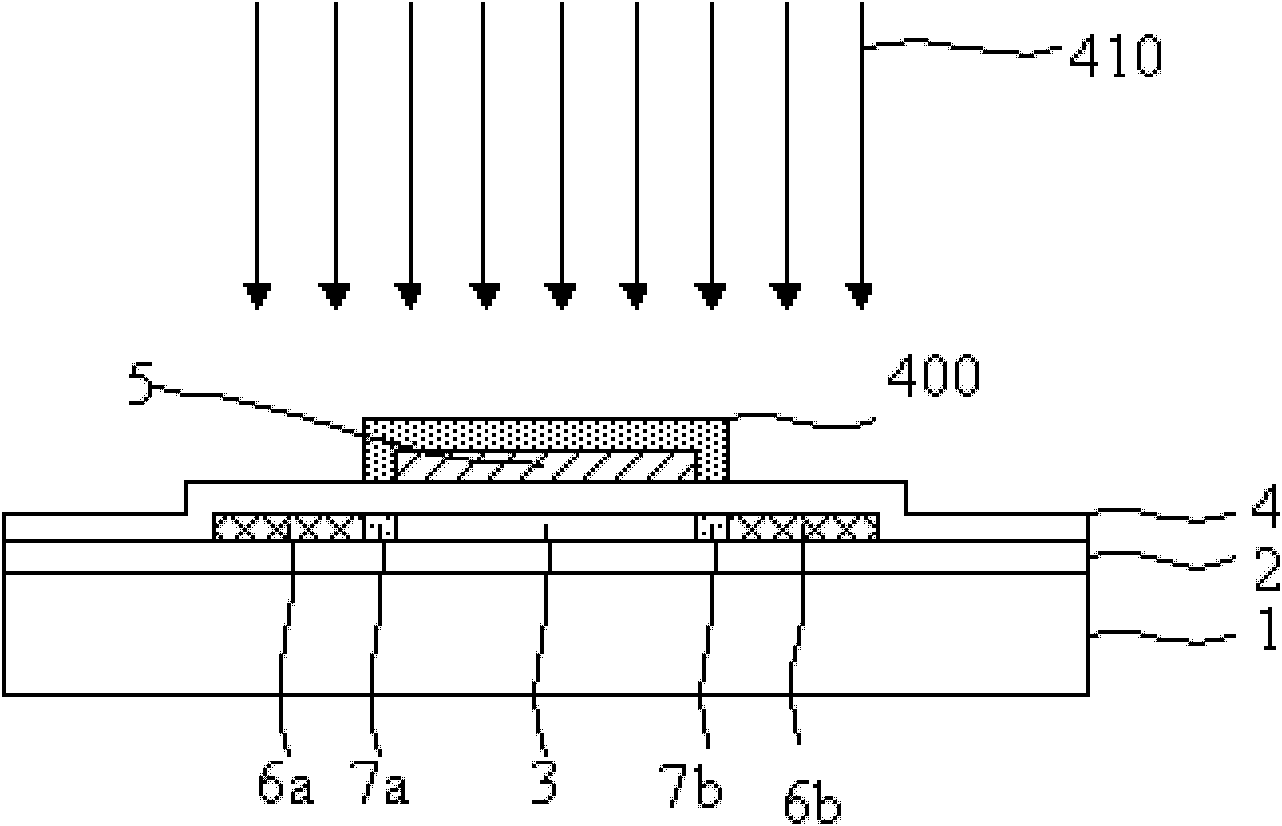
[0040] The auxiliary layer 910 is formed on the gate conductive layer 510 according to the method of the first embodiment, wherein the auxiliary layer 910 and the gate insulating layer 4 use the same film material and the same manufacturing process. The thickness of the auxiliary layer 910 determines the dopant dose of the lightly doped region, and its thickness is between between. A better example uses silicon nitride as the gate insulating layer. At this time, the auxiliary layer is also silicon nitride. The way to form silicon nitride is to use PECVD process, the reaction gas is SiH4 / NH3, and the optimized auxiliary layer thickness is

[0041] After the LDD formation layer 9 is formed according to the method of Embodiment 1, the photoresist is not removed, and the gate conductive layer 510 is over-etched by a wet method to form the gate 5. The width of the gate is smaller than the width of the photoresist pattern, and the optimized photoresist The width of the pattern i...

Embodiment 3

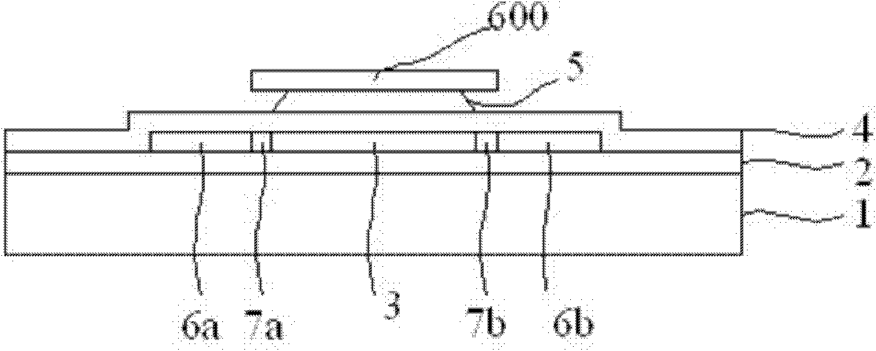
[0044] A manufacturing method of a thin film transistor according to another embodiment includes the following steps.

[0045] The auxiliary layer 910 is formed on the gate conductive layer 510 according to the method of the first embodiment, wherein the auxiliary layer 910 and the gate insulating layer 4 adopt the same film material and the same manufacturing process. The thickness of the auxiliary layer 910 determines the dopant dose of the lightly doped region, and its thickness is between between. A better example uses silicon nitride as the gate insulating layer. At this time, the auxiliary layer is also silicon nitride. The method of forming silicon nitride is PECVD process, and the reaction gas is SiH4 / NH3. The optimized auxiliary layer thickness and gate insulating layer The same thickness, both

[0046] After the LDD formation layer 9 is formed according to the method of Embodiment 1, the photoresist is not removed, and the gate conductive layer 510 is over-etche...


PUM


Abstract

The invention discloses a manufacturing method of a thin film transistor and a transistor manufactured by the method, wherein the method is characterized by comprising the following steps: sequentially forming a surface covering layer, a polycrystalline silicon island active layer, a grid insulating layer, a grid electrode conducting layer and an auxiliary layer on a baseplate, photoetching the auxiliary layer to form an LDD forming layer, and forming a lightly doped drain electrode region, a heavily doped source electrode, a heavily doped drain electrode and a channel on the polycrystalline silicon island active layer by utilizing the action of the LDD forming layer and through only once doped ion implantation. The method of the invention only needs once ion implantation, simplifies the manufacturing working procedures and lowers the manufacturing cost; the thin film transistor which is manufactured by adopting the method and provided with a lightly doped drain electrode has the advantages of small electrode area and large numerical aperture.

Description

technical field [0001] The invention relates to the field of low temperature polysilicon thin film transistor manufacturing, in particular to a method for manufacturing a thin film transistor with lightly doped drain electrodes and a transistor manufactured by the method. Background technique [0002] Compared with traditional amorphous silicon (α-Si) thin film transistors, low temperature polysilicon thin film transistors (LTPS TFTs) have higher electron mobility, fast response speed, short image data writing time, and are easy to realize large-area video display. In addition, polysilicon also has the characteristics of poor photosensitivity; stable operation; good transparency; self-alignment can be realized in the process; peripheral driving circuit and display area can be integrated and integrated, which solves the problem of excessive leads and difficulty in α-Si TFT technology. A series of problems such as automatic detection make the application of polysilicon TFT in ...

Claims


Application Information

Patent Timeline
Patent Type & Authority Applications(China)
IPC IPC(8): H01L21/336H01L21/265H01L29/786
Inventor 刘萍
Owner SHENZHEN DANBANG INVESTMENT GROUP
Why Eureka
Try Eureka