
Method for preparing high-orientation PZT piezoelectric thin film

A piezoelectric film and high orientation technology, which is applied in the field of preparation of high orientation PZT piezoelectric film, can solve the problems of low perovskite phase ratio and difficulty in forming crystallization nuclei

Inactive Publication Date: 2010-10-20
冯士维 +1
View PDF0 Cites 3 Cited by
  • Summary
  • Abstract
  • Description
  • Claims
  • Application Information

AI Technical Summary

Problems solved by technology

Therefore, for the zirconium-rich PZT (~70 / ~30) film, on the one hand, due to the large mismatch between its lattice constant and the lattice constant of the transition metal phase produced during the crystallization process, it is not easy to form a crystallization nucleus; on the other hand, due to The pre-baking temperature is relatively low, so the proportion of perovskite phase is low

Method used


Image

  • Method for preparing high-orientation PZT piezoelectric thin film
  • Method for preparing high-orientation PZT piezoelectric thin film

Examples


Embodiment 1

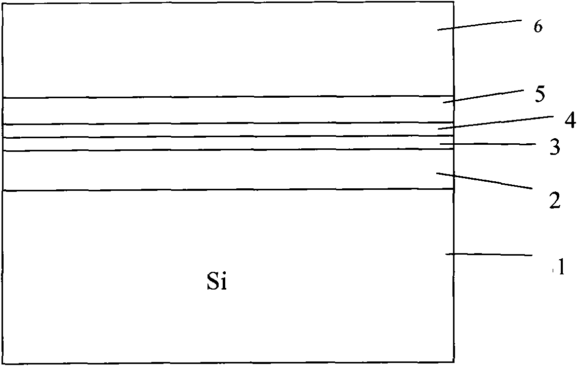
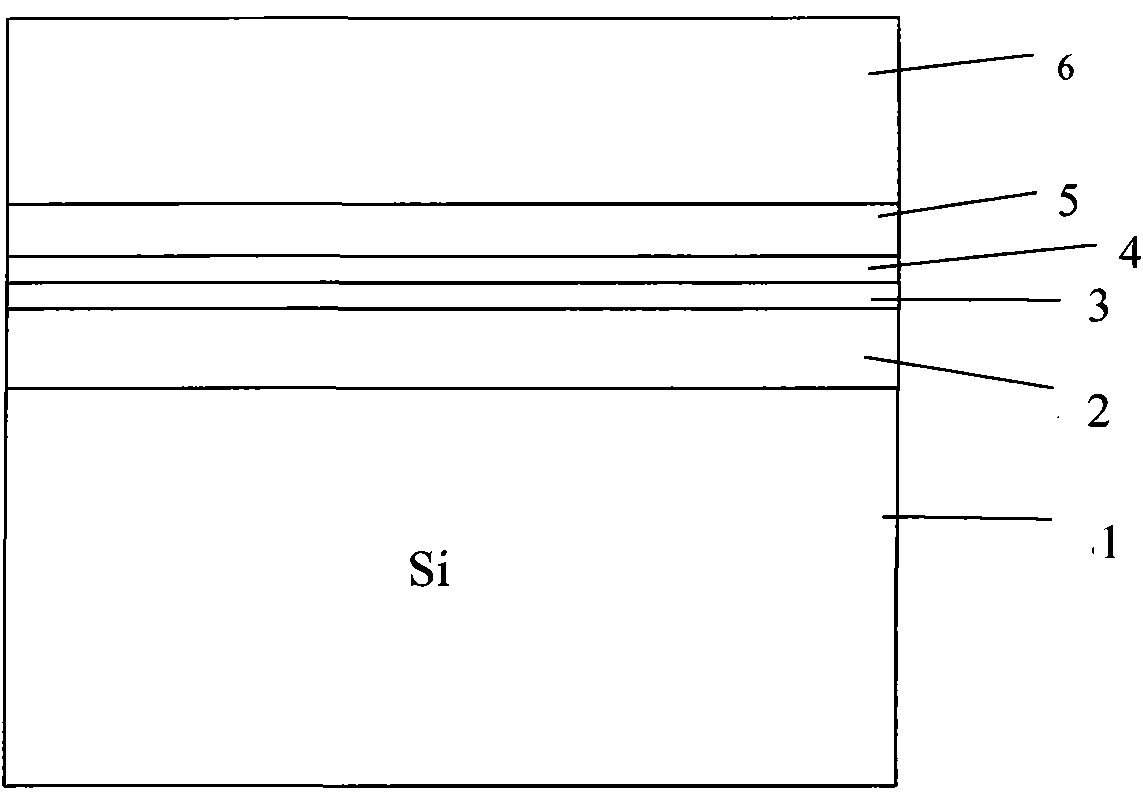
[0019] The Si wafer is cleaned by the conventional cleaning method of the Si wafer in the IC industry, and SiO is grown on the silicon wafer by thermal growth method. 2 The thickness of the layer is 1 μm, and then a Ti layer of 10 nm is deposited by sputtering or CVD, and a Pt layer of 100 nm is deposited by sputtering or CVD, and the growth of the PZT layer adopts a two-step method. That is, MOCVD or sputtering is used to slowly grow a PT seed layer (seed layer) of 50 nm, and then increase the sputtering rate to grow or spin coat a PZT layer.

[0020] After the PT grows and before the PZT, the PT layer is subjected to a rapid annealing process (RTP) once. During the growth of the PZT layer, a rapid annealing process (RTP) is performed every 300nm

Embodiment 2

[0022] The Si wafer is cleaned by the conventional cleaning method of the Si wafer in the IC industry, and SiO is grown on the silicon wafer by thermal growth method. 2 The thickness of the layer is 0.5um, and then sputtering method or CVD method is used to deposit TiO, Ti layers are 75nm and 100nm respectively, and then sputtering method or CVD method is used to deposit Pt layer 100nm, and the growth of PZT layer adopts two-step method. That is, the sputtering method is used to slowly grow the PT seed layer (seed layer) 50nm, and then increase the sputtering rate to grow or spin-coat the PZT layer.

[0023] After the PT grows and before the PZT, the PT layer is subjected to a rapid annealing process (RTP) once. During the growth of the PZT layer, a rapid annealing process (RTP) is performed every 300nm


PUM


Abstract

The invention discloses a method for preparing a high-orientation PZT piezoelectric thin film. The method is characterized by comprising the following steps of: sequentially growing a SiO2 layer, a Ti layer, a Pt layer, a PbTiO3 layer, a PZT layer (spin coating or sputtering) and a top electrode layer on a silicon wafer, wherein the PbTiO3 layer is abbreviated as a PT layer, used as a seed crystal layer or a seed layer and made by MOCVD, sputtering or MBE method; and performing rapid annealing process (RTP) on the PT layer and the PZT layer once or several times during the growth of the PT and PZT. Compared with a conventional silicon / silicon dioxide / Pt / PZT / top electrode structure, the PZT piezoelectric thin film prepared by the method has the advantages of high preferred orientation and high electro-mechanical coupling coefficient.

Description

technical field [0001] The invention relates to a preparation method of a PZT piezoelectric film with a high degree of orientation Background technique [0002] PZT piezoelectric thin film material has a large electromechanical coupling coefficient (K 2 is 20.25%), can be used in non-volatile memory and micro-electromechanical devices, and is easy to integrate with Si, which has aroused great interest in its research. PZT thin films can also be prepared by sputtering, PLD and other methods, but the commonly used preparation method is the sol-gel method. It is a low-cost film-making method, which has the advantages of easy control of film components, compact structure, easy large-area film formation, and compatibility with IC technology. It is currently widely used in the preparation of PZT thin films in MEMS technology. The sol-gel method can obtain good film properties, but the film thickness is not easy to control, the repeatability is poor, and the performance needs to ...

Claims


Application Information

Patent Timeline
IPC IPC(8): C23C28/00C23C14/34C23C16/44C23C14/06
Inventor 冯士维钟素娟
Owner 冯士维
Learn More