Light-emitting diode chip and manufacturing method thereof

A technology of light-emitting diodes and manufacturing methods, which is applied in the direction of electrical components, circuits, semiconductor devices, etc., can solve the problems of GaN-based LED epitaxial layer damage, affecting LED optical and electrical properties, and expensive equipment, so as to improve light extraction efficiency and solve Dissipate heat and light, improve the effect of recombination efficiency

Inactive Publication Date: 2010-10-27
刘胜
View PDF4 Cites 36 Cited by
  • Summary
  • Abstract
  • Description
  • Claims
  • Application Information

AI Technical Summary

Problems solved by technology

The GaN-based LED epitaxial layer can be transferred to other substrates with high electrical conductivity and high thermal conductivity (such as Si, Cu and Al) by using the combination of laser lift-off technology and bonding technology, thereby eliminating the impact of the sapphire substrate on the GaN-based substrate. Adverse effects brought by LED, but this technology has the following problems: (1) The use of laser to lift off the sapphire substrate is easy to cause damage to the GaN-based LED epitaxial layer, which affects the optical and electrical properties of the LED
(3) Laser lift-off technology is not compatible with the old process, and the equipment is expensive

Method used


Image

  • Light-emitting diode chip and manufacturing method thereof
  • Light-emitting diode chip and manufacturing method thereof
  • Light-emitting diode chip and manufacturing method thereof

Examples


Embodiment Construction

[0031] Embodiments of the present invention are further described below in conjunction with the accompanying drawings:

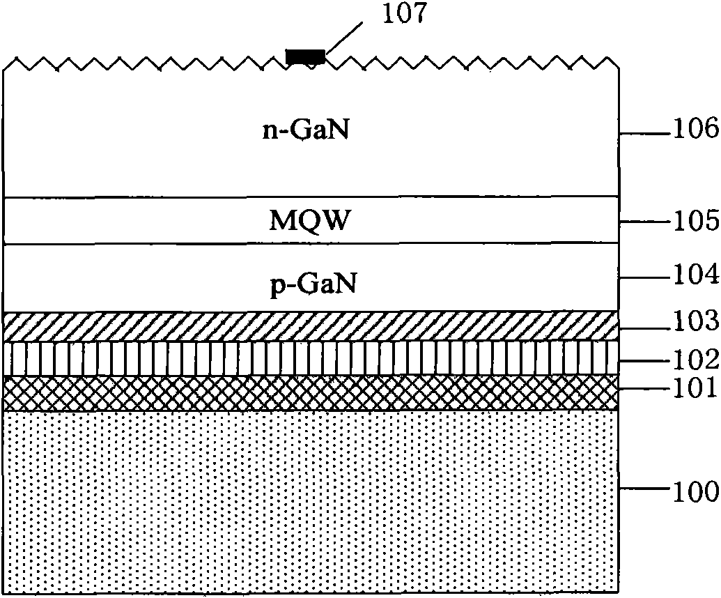
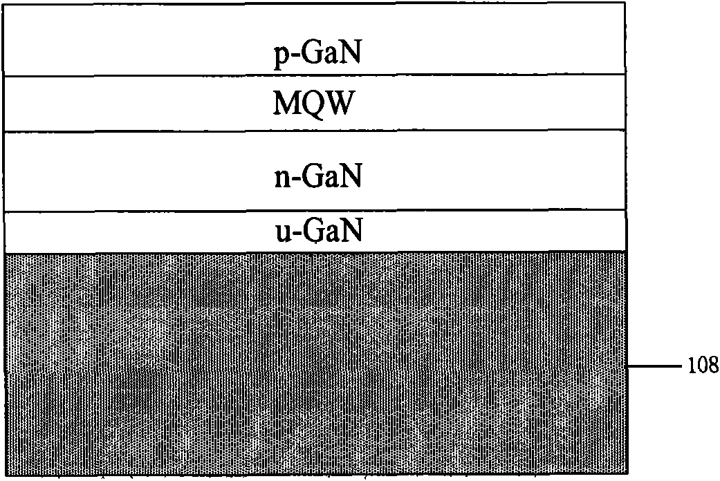
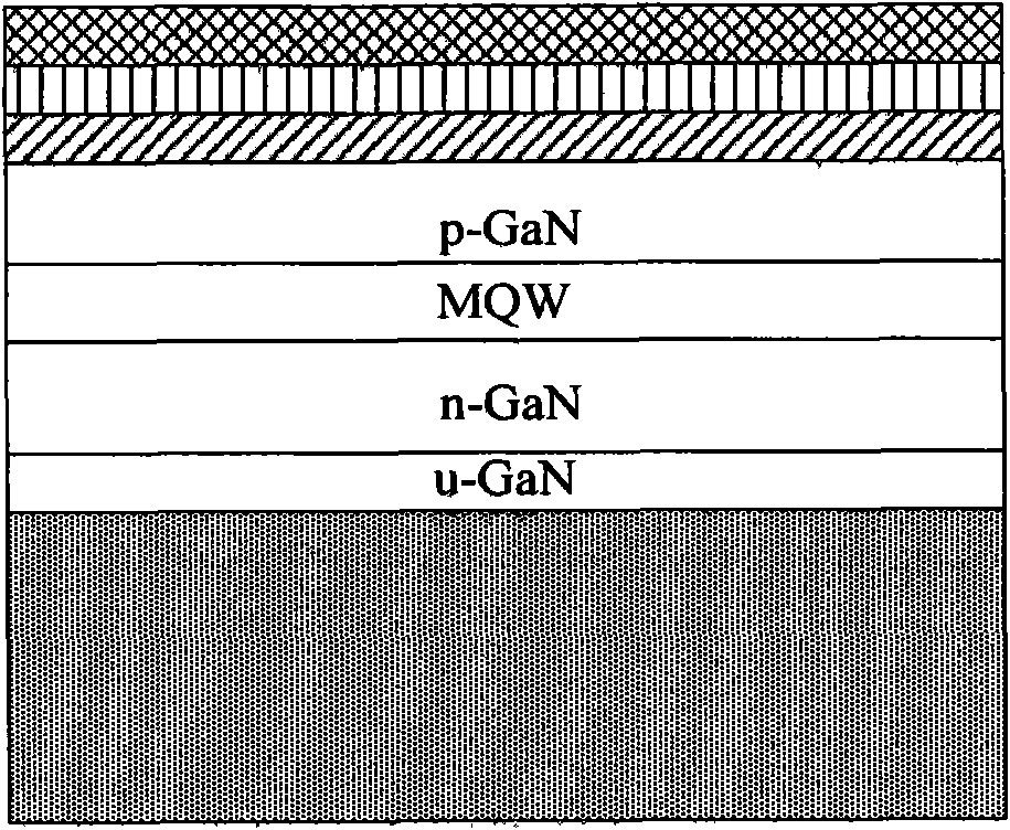
[0032] The present invention adopts high thermal conductivity material as the support substrate 100 of the vertical light-emitting diode (LED) chip, and the high thermal conductivity substrate 100 is above the bonding material layer 101, and its material is a conductive polymer, and above the bonding material layer 101 is Reflective layer 102, its material is Al or Ag or Pt, and above reflective layer 102 is transparent conductive layer 103, and its material is ITO or ATO or ZnO, and transparent conductive layer 103 is above p-GaN layer 104, and above p-GaN layer 104 It is the active layer 105, the active layer 105 is above the n-GaN layer 106, and the n-GaN layer 106 is above the ohmic contact electrode 107, and the ohmic contact electrode 107 is Ti / Al / Ti / Au or Cr / / Pt layer by layer / Au or Ti / Al / Pt / Au. Fabricate a transparent conductive layer 103 and a ref...


PUM

PropertyMeasurementUnit
thicknessaaaaaaaaaa
thicknessaaaaaaaaaa
thicknessaaaaaaaaaa

Abstract

The invention relates to a light-emitting diode (LED) chip and a manufacturing method thereof. Materials with high heat conductivity are used as a support substrate of the LED chip, and the support substrate is sequentially provided with a bonding material layer, a reflecting layer, a transparent electrode layer, an epitaxial layer and an n-surface electrode. The manufacturing method comprises the following steps of: coating a transparent conducting layer on a sapphire substrate GaN epitaxial wafer by vaporization; coating the reflecting layer on the conducting layer by vaporization; spreading the bonding material layer on the reflecting layer, and bonding the sapphire substrate GaN epitaxial wafer to the substrate; removing the sapphire substrate by combining mechanical grinding, chemical mechanical polishing and wet-method corrosion; etching an n-GaN, an active layer and a p-GaN by using inductively coupled plasmas, removing the undoped GaN layer by etching with a potassium hydroxide solution, and coarsening the surface of the n-GaN; and coating the n-surface electrode to the n-GaN layer by vaporization to form an ohmic contact. The invention avoids the damage to the GaN-based LED epitaxial layer and the bonding layer caused by the stripping of the sapphire substrate by using laser, and the heat radiation efficiency is improved by using the substrate with high heat conductivity.

Description

technical field [0001] The invention relates to a chip of a light emitting diode and a manufacturing method thereof, in particular to a chip of a light emitting diode manufactured by an integrated mechanical grinding, chemical mechanical polishing and wet etching stripping method and a manufacturing process thereof. Background technique [0002] GaN-based blue and blue-green light-emitting diodes (LEDs) are widely used in instrument indicators, large-size LED backlights, electronic billboards, and various lighting equipment. Due to the limitations of GaN crystal structure and growth conditions, sapphire is mainly selected as the substrate when growing GaN-based LED epitaxial layers. Due to the poor electrical and thermal conductivity of sapphire, the manufacturing process of GaN-based LEDs is complicated, the heat dissipation is poor, and the lifespan is short, which limits the application of high-brightness LEDs. For GaN-based LED chips with horizontal electrode structure,...

Claims


Application Information

Patent Timeline
Patent Type & Authority Applications(China)
IPC IPC(8): H01L33/00
Inventor 刘胜甘志银汪沛周圣军
Owner 刘胜
Why Eureka
Try Eureka