GaN-based LED having nanometer structure inserted layer

A nanostructure and intercalation technology, applied in electrical components, circuits, semiconductor devices, etc., can solve problems such as thermal effects, P-type damage, and difficulty in making ohmic contacts

Inactive Publication Date: 2010-10-27
INST OF SEMICONDUCTORS - CHINESE ACAD OF SCI
View PDF3 Cites 8 Cited by
  • Summary
  • Abstract
  • Description
  • Claims
  • Application Information

AI Technical Summary

Problems solved by technology

However, these methods are relatively complicated to operate, which brings more or less problems to the subsequent growth and process manufacturing. For example, surface roughening may cause damag...

Method used


Image

  • GaN-based LED having nanometer structure inserted layer
  • GaN-based LED having nanometer structure inserted layer
  • GaN-based LED having nanometer structure inserted layer

Examples


Embodiment Construction

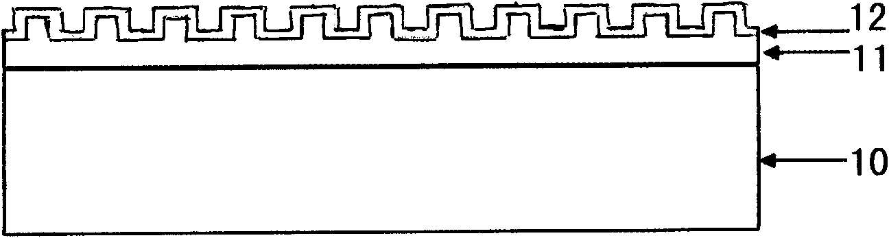
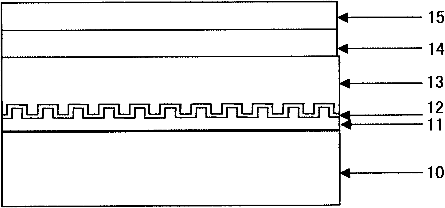
[0027] The present invention provides a GaN-based LED with a nanostructure insertion layer, comprising:

[0028] A substrate 10, the substrate 10 is made of silicon, sapphire, gallium nitride, gallium arsenide or silicon carbide;

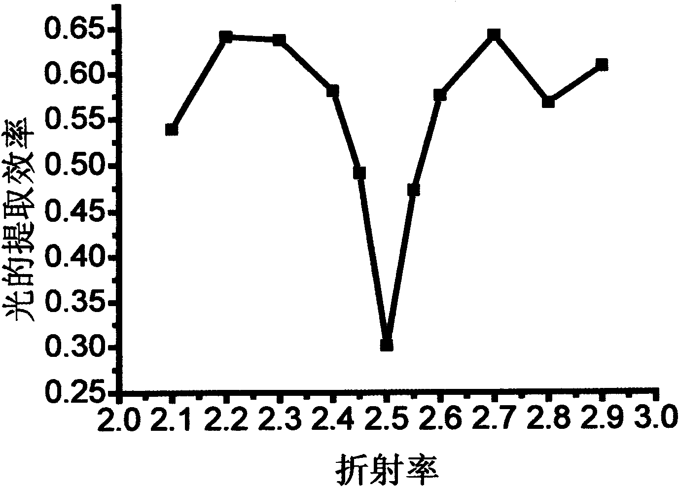
[0029] A nanostructure template 11, the nanostructure template 11 is epitaxially grown on the substrate 10, the surface of the nanostructure template 11 is in a concave-convex shape, and the nanostructure template 11 on the concave-convex surface is obtained by electron beam exposure, holographic lithography, and two The porous alumina structure formed by step oxidation, the self-organized structure formed by metal under annealing conditions or the structure formed by silica nanoparticles is used as a mask to etch by dry etching method, or directly etched by focused ion beam wherein the surface of the nanostructure template 11 is a columnar structure, and the shape is a cylinder, a hexagonal prism, a square prism, a rhombus prism, a cubic prism, a t...


PUM

PropertyMeasurementUnit
Heightaaaaaaaaaa
Sizeaaaaaaaaaa
Thicknessaaaaaaaaaa

Abstract

A GaN-based LED having a nanometer structure inserted layer comprises a substrate and a nanometer structured template, wherein the nanometer structured template is epitaxially grown on the substrate and the surface thereof is of a concave-convex shape. The LED further comprises an inserted layer which is epitaxially grown on the nanometer structured template, an N-type ohmic contact layer which is epitaxially grown on the inserted layer and one side on which is provided with a table-board, an active layer which is epitaxially grown on the other side of the table-board of the N-type ohmic contact layer, a P-type layer is epitaxially grown on the active layer, a transparent electrode layer which is made on the P-type layer, a P bonding electrode which is photo-etched on the P-type and an N ohmic contact electrode 22 which is made on the table-board of the N-type ohmic contact layer.

Description

technical field [0001] The invention belongs to the field of semiconductor devices, in particular to a GaN-based LED with a nanostructure insertion layer. Background technique [0002] As a new generation of lighting sources, GaN-based LEDs have the advantages of energy saving and environmental protection, and can be widely used in various indications, displays, decorations, backlights, general lighting and urban night scenes. However, due to the large difference in refractive index between the GaN material and the epoxy resin used for packaging, the epoxy resin and air, the internal total reflection critical angle is very small (only 23.6°). Because of total reflection, a large amount of light cannot exit from the interface, and because the upper and lower interfaces are parallel, the light that cannot exit for the first time will propagate repeatedly in the dielectric material until all the light energy is dissipated into heat energy. This is not conducive to the utilizat...

Claims


Application Information

Patent Timeline
IPC IPC(8): H01L33/20H01L33/22
Inventor 朱继红张书明朱建军
Owner INST OF SEMICONDUCTORS - CHINESE ACAD OF SCI
Why Eureka
Try Eureka