Resistor-type nonvolatile storage device and manufacturing method thereof

A non-volatile storage, resistive technology, applied in static memory, digital memory information, electrical components, etc.

Inactive Publication Date: 2010-10-27
INST OF MICROELECTRONICS CHINESE ACAD OF SCI
View PDF0 Cites 15 Cited by
  • Summary
  • Abstract
  • Description
  • Claims
  • Application Information

AI Technical Summary

Problems solved by technology

[0005] Although the resistance transition phenomenon of this type of solid electrolyte material based on the electrochemical reaction mechanism has been well explained, the formation of conductive filaments is a random process, resulting in a large discreteness in the relevant electrical characteristics of the device. (eg programming voltage)

Method used


Image

  • Resistor-type nonvolatile storage device and manufacturing method thereof
  • Resistor-type nonvolatile storage device and manufacturing method thereof
  • Resistor-type nonvolatile storage device and manufacturing method thereof

Examples


Embodiment Construction

[0035] In order to make the object, technical solution and advantages of the present invention clearer, the present invention will be described in further detail below in conjunction with specific embodiments and with reference to the accompanying drawings.

[0036] The process steps of the present invention to make the resistive non-volatile memory device are as follows:

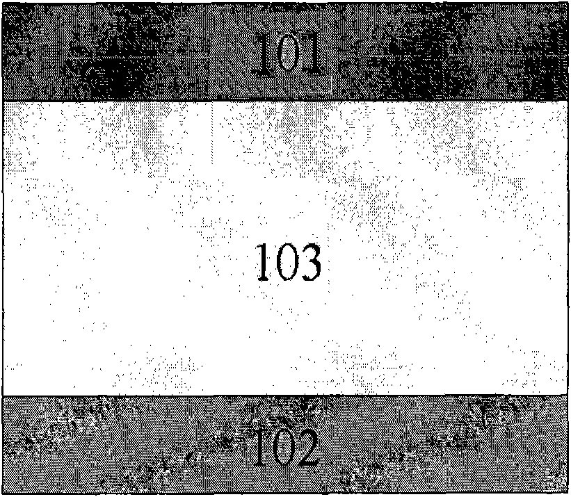
[0037] 1) Using electron beam evaporation or magnetron sputtering to deposit conductive electrode metal on the insulating substrate, the thickness of the metal electrode layer is 100-500nm;

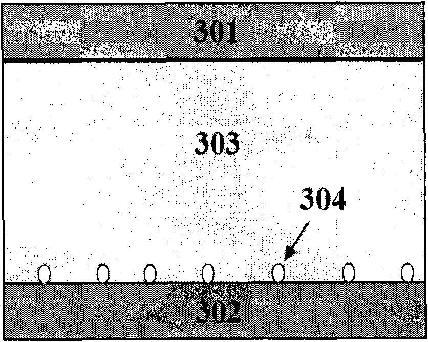
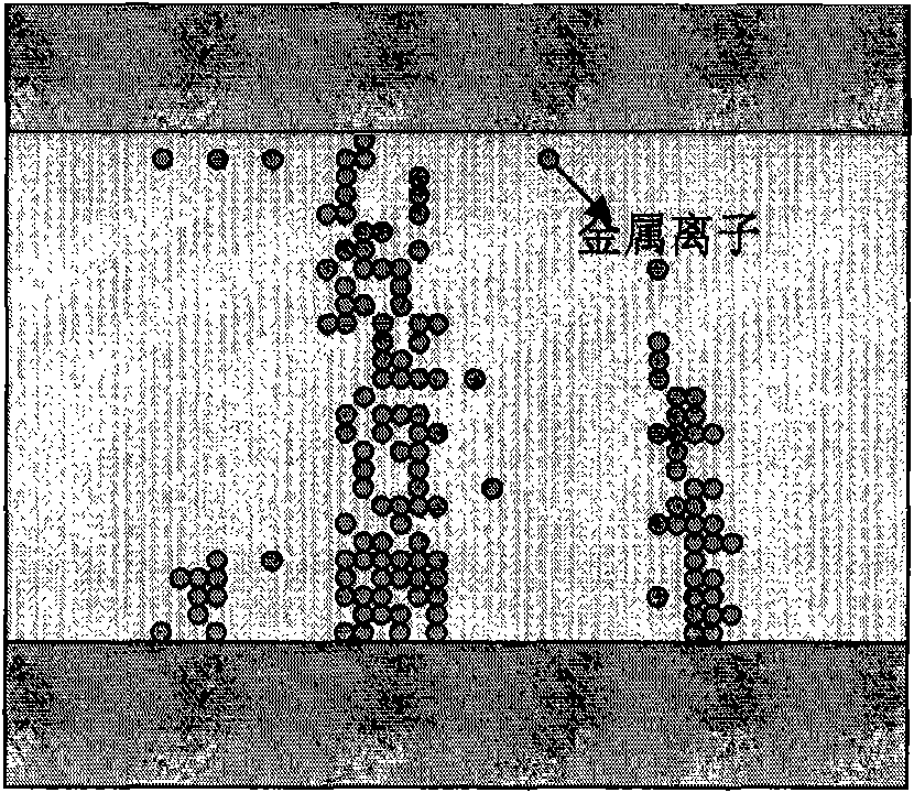
[0038] 2) Deposit a metal film with a thickness of several nm on the lower conductive electrode material by means of evaporation, sputtering, atomic layer deposition, etc., and then form the metal nanocrystal by rapid thermal annealing or high temperature thermal annealing; or use sol -Gel method to form metal nanocrystals. The specific operation method is to transfer the solution containing metal nanocrystal particles...


PUM

PropertyMeasurementUnit
thicknessaaaaaaaaaa
diameteraaaaaaaaaa
thicknessaaaaaaaaaa

Abstract

The invention discloses a resistor-type nonvolatile storage device, comprising an upper conducting electrode, a lower conducting electrode, a solid-state electrolyte film or a binary oxide film, and metal nanocrystalline, wherein the solid-state electrolyte film or the binary oxide film is contained between the upper conducting electrode and the lower conducting electrode; and the metal nanocrystalline is positioned on the upper surface of the lower conducting electrode. The invention discloses a method for manufacturing the resistor-type nonvolatile storage device simultaneously. Aiming at the current situation that the randomness in the formation process of a conducting channel exists in two categories, i.e. fuse/antifuse and ion conduction-type in a resistor transitional type storage at present, the invention changes the electric-field strength in local parts by changing the appearance for the lower conducting electrode, thus achieving the purpose of controlling the formed position of the conducting channel. The resistor transitional type storage manufactured by the method has the characteristics of low programming voltage, little discreteness of the programming voltage, low power consumption, fast programming speed and the like.

Description

technical field [0001] The invention belongs to the technical field of microelectronic devices and memories, and in particular relates to a resistive nonvolatile memory device capable of controlling the growth position of conductive filaments and a manufacturing method thereof. Background technique [0002] In recent years, the explosive growth of the 3C consumer electronics market has led to a rapid increase in the market demand for non-volatile memory. Flash memory (flash memory) is currently the dominant non-volatile memory, and its output value will approach that of DRAM. However, the traditional Flash memory is a silicon-based non-volatile memory based on a polysilicon thin-film floating gate structure, and this structure is facing the challenge of how to keep shrinking. According to the International Semiconductor Technology Development Roadmap (ITRS) in 2005, the traditional polysilicon floating gate memory can only continue to the 65nm technology node. Therefore, i...

Claims


Application Information

Patent Timeline
Patent Type & Authority Applications(China)
IPC IPC(8): H01L45/00G11C11/56
Inventor 刘明刘琦龙世兵王艳张森
Owner INST OF MICROELECTRONICS CHINESE ACAD OF SCI
Why Eureka
Try Eureka