Ceramic sputtering target assembly and seaming method thereof

A technology of sputtering target and ceramics, which is applied in the direction of sputtering coating, ceramic layered products, chemical instruments and methods, etc. It can solve the problems of abnormal growth of target grains and achieve the effect of tight bonding

Active Publication Date: 2010-11-10
SOLAR APPLIED MATERIALS TECHNOLOGY CORPORATION
View PDF4 Cites 25 Cited by
  • Summary
  • Abstract
  • Description
  • Claims
  • Application Information

AI Technical Summary

Problems solved by technology

[0006] U.S. Patent Publication No. US 2003/0129407 discloses sputtering titanium (Ti) or chromium (Cr) on the substrate to improve the adhesion between the graphite film on the substrate surface and the substrate. However, this patent only discloses Properties of Thin Film Materials
[0007] In U.S. Patent No. US6,555,250, it was disclosed in detail that nickel (Ni) electroplating was carried out on the surface of the metal target, and that the...

Method used


Image

  • Ceramic sputtering target assembly and seaming method thereof
  • Ceramic sputtering target assembly and seaming method thereof
  • Ceramic sputtering target assembly and seaming method thereof

Examples


Embodiment 1

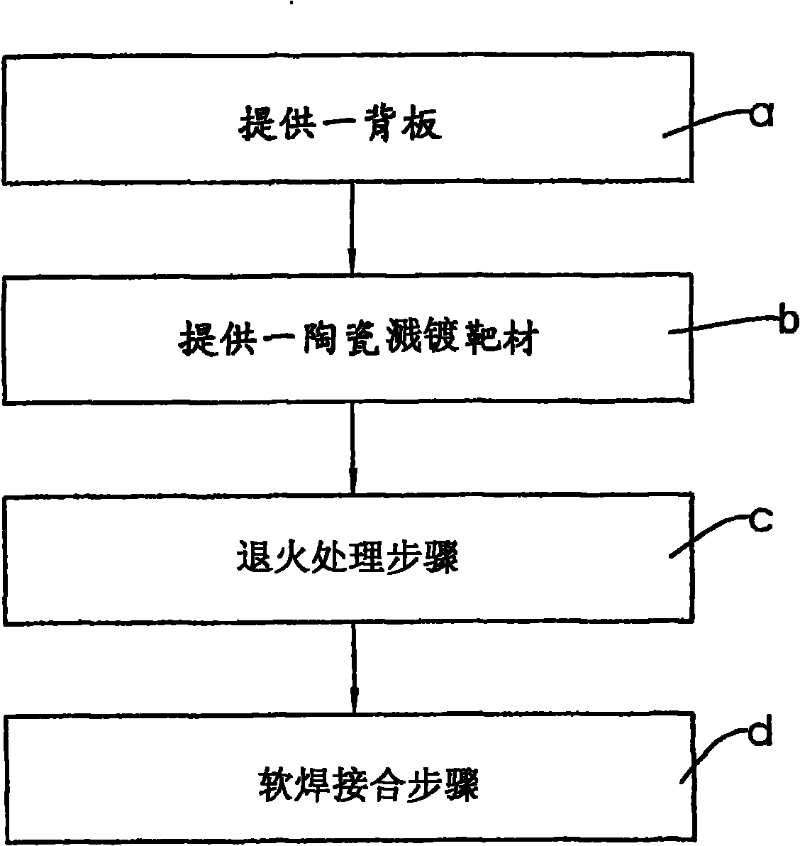
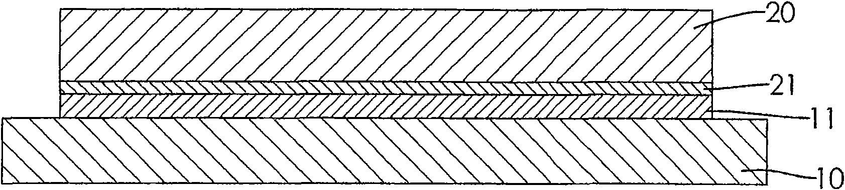
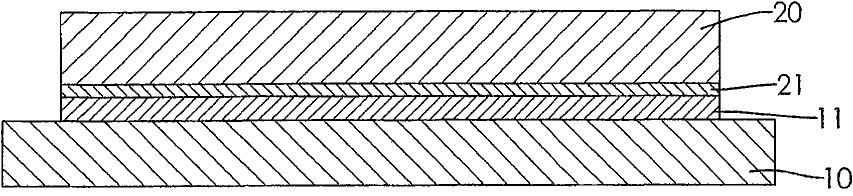
[0044] Coat one surface of the copper back plate with indium solder with low melting point to form a soft solder layer, and heat it to make it into a molten state (the melting point of indium is 156.6°C); vapor-deposit pure chromium material on the surface of the graphite target, and the thickness of the coating film is 1 μm; put the entire target into a vacuum heating furnace for temperature of 1200 ° C ~ 1500 ° C and pressure at 10 -5 to 10 -1The annealing treatment of torr, the treatment time is not more than 3 hours; after the target is annealed, the peeling test is carried out with cellophane tape to determine the peeling of the chromium-free coating, and then the target with chrome plating The surface of the target is treated with ultrasonic wet coating of indium solder, and finally the surface and the molten solder layer of the copper back plate are soldered and bonded, and the temperature is lowered to complete the welding of the target and the back plate. Follow-up a...

Embodiment 2

[0046] Coat one surface of the copper back plate with low-melting indium solder to form a soft solder layer, and heat it to make it into a molten state (the melting point of indium is 156.6°C); vapor-deposit pure chromium on the surface of the ITO (Indium Tin Oxide) target material, the coating thickness is 1 μm; the entire target is placed in a vacuum heating furnace at a temperature of 900°C to 1100°C and a pressure of 10 -5 to 10 -1 The annealing treatment of torr, the treatment time is not more than 3 hours; after the target is annealed, the peeling test (peeling test) is carried out with Sailufan tape to confirm that the chrome-free coating is peeled off, and then super-indium solder is carried out on the surface of the chrome-plated target. Sonic wet coating treatment, and finally the surface and the molten solder layer of the copper back plate are soldered and bonded, and the temperature is lowered to complete the welding of the target and the back plate. Follow-up and...

Embodiment 3

[0048] Coat one surface of the copper back plate with low-melting indium solder to form a soft solder layer, and heat it to make it into a molten state (the melting point of indium is 156.6°C); evaporate 95wt% of the surface of the ITO (Indium Tin Oxide) target Chromium-5wt% gold material, the coating thickness is 5μm; the whole target is placed in a vacuum heating furnace at a temperature of 900°C to 1100°C and a pressure of 10 -5 to 10 -1 The annealing treatment of torr, the treatment time is not more than 3 hours; after the target is annealed, the peeling test (peeling test) is carried out with Sailufan tape to determine the peeling of the chrome-gold plating layer, and then the surface of the target with chrome-gold plating is carried out Ultrasonic wet coating treatment of indium solder, and finally the surface and the molten solder layer of the copper back plate are soldered and bonded, and the temperature is lowered to complete the welding of the target and the back pla...


PUM

PropertyMeasurementUnit
Thicknessaaaaaaaaaa
Thicknessaaaaaaaaaa
Thicknessaaaaaaaaaa

Abstract

The invention provides a seaming method for a ceramic sputtering target, which comprises the following steps: providing a back board and forming a soft solder layer with lower melting point solder on the surface of the back board; providing a ceramic sputtering target, and forming an interface layer on the surface by filming treatment of pure chromium or chromium alloy; carrying out annealing treatment on the ceramic sputtering target with the interface layer; and carrying out soft soldering joint on the solder layer of the back board and the interface layer of the target. In the invention, after the chromium or chromium alloy interface layer is formed on the ceramic sputtering target, and annealing treatment is carried out on the interface layer, excellent joint adhesive capacity is formed between the interface layer and the soft solder layer, thus the ceramic sputtering target and the back board are jointed more tightly.

Description

technical field [0001] The invention relates to a sputtering target component and its welding method, in particular to a ceramic sputtering target component and its soldering method. Background technique [0002] Carbon, silicon or ceramic targets are mostly used to form transparent conductive oxides in liquid crystal displays or touch panels, such as indium tin oxide (ITO) targets or DLC graphite coatings (diamond-like carbon) in hard disks. coating). At present, the welding of such targets mostly adopts the method of soft soldering. [0003] In the general industry, when performing the welding process of carbon, silicon or ceramic sputtering targets, the most commonly used method is solder bonding with the copper backplane, and the solder used is indium (In) with a low melting point. or tin (Sn) material. The advantage of the soldering bonding method is that the processing temperature is low (usually less than 250°C), and it will not cause the subsequent abnormal grain ...

Claims


Application Information

Patent Timeline
IPC IPC(8): B23K1/00B23K1/20C21D1/26C21D1/74C21D11/00C23C14/18C23C14/24C23C14/34B32B15/04B32B18/00
Inventor 吴国贤杜承鑫
Owner SOLAR APPLIED MATERIALS TECHNOLOGY CORPORATION
Why Eureka
Try Eureka