Method and device for removing barrier layer

A technology of barrier layer and metal layer, used in electrical components, semiconductor/solid-state device manufacturing, circuits, etc., can solve problems such as damage to copper, etching, etc.

Active Publication Date: 2010-11-10
ACM RES SHANGHAI
View PDF9 Cites 38 Cited by
  • Summary
  • Abstract
  • Description
  • Claims
  • Application Information

AI Technical Summary

Problems solved by technology

However, NaOH / H 2 o 2 and KOH / H 2 o 2 To a certain extent, it will etch and damage the copper in the slot

Method used


Image

  • Method and device for removing barrier layer
  • Method and device for removing barrier layer
  • Method and device for removing barrier layer

Examples


Embodiment Construction

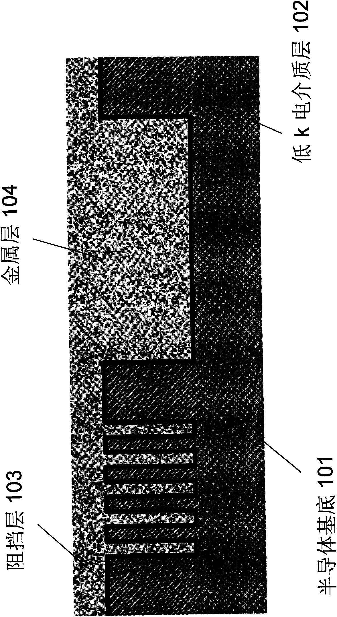
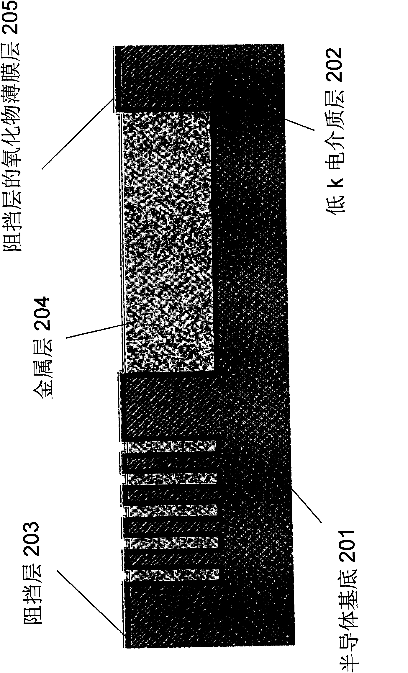
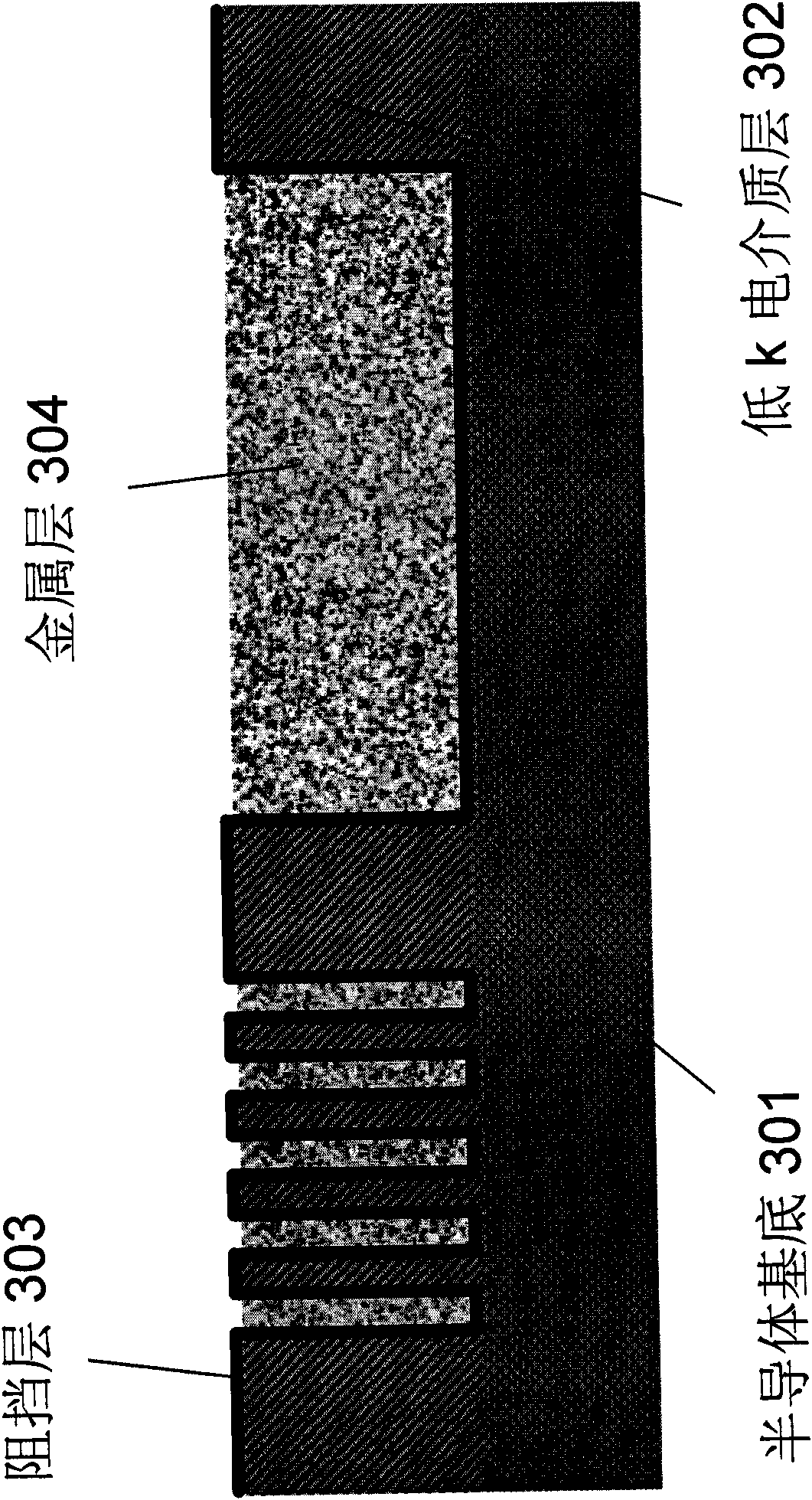
[0024] The present invention relates to a semiconductor device processing method and device. More specifically, the present invention relates to removing or etching barrier layers, such as tantalum / tantalum nitride, suitable for low-k dielectric materials. This facilitates various applications of low-k materials in semiconductor devices.

[0025] Figure 1 to Figure 4 Shown is the combination of some new processes in semiconductor processing: copper removal by stress-free polishing, etchant to remove tantalum oxide formed on the surface of the barrier layer during copper polishing, and selective xenon difluoride gas The barrier layer tantalum / tantalum nitride is removed by etching. Among them, no matter the electrochemical copper throwing, the removal of tantalum oxide, or the etching barrier layer of xenon difluoride are all processes without mechanical force. This set of processes thus minimizes mechanical damage to the semiconductor structure, minimizes blanketing effect...


PUM


Abstract

The invention relates to a method and device for integrating an unstressed electrochemical polishing process for copper interconnection for semiconductor manufacturing, a process for removing a tantalum or titanium oxide film formed in an unstressed polishing process and a process for etching a barrier layer tantalum / tantalum nitride or titanium / titanium nitride by using a xenon difluoride gas phase. The method comprises the following steps of: firstly, removing at least part of copper which is plated on a silicon plate by unstressed electrochemical polishing; secondly, removing the tantalum or titanium oxide film formed on the surface of the barrier layer in the copper-removal polishing process; and finally, removing the barrier layer tantalum / tantalum nitride or titanium / titanium nitride by xenon difluoride gas-etching. The device consists of three sub-systems, namely an unstressed electrochemical copper polishing system, a system for removing the tantalum or titanium oxide film on the surface of the barrier layer by using etchant and a xenon difluoride gas-etching system for removing the barrier layer.

Description

technical field [0001] This invention relates to semiconductor processing methods and apparatus. Specifically, it is about stress-free copper polishing and selective removal of barrier layers. More specifically, the present invention relates to processes that can be used to selectively polish copper and stress-free removal of tantalum / tantalum nitride barrier layers in integrated device fabrication. Background technique [0002] Semiconductor devices are formed by forming transistors and interconnection lines on semiconductor silicon wafers through a series of different processing steps. In order for the transistor terminals to be connected to the silicon chip, conductive (eg metal) slots, holes and the like need to be made in the dielectric material of the silicon chip as part of the device. Slots and holes can transfer electrical signals and energy between transistors, internal circuits, and external circuits. [0003] When forming interconnect elements, semiconductor s...

Claims


Application Information

Patent Timeline
Patent Type & Authority Applications(China)
IPC IPC(8): H01L21/768H01L21/321H01L21/311H01L21/00
Inventor 王坚贾照伟武俊萍谢良智王晖
Owner ACM RES SHANGHAI
Why Eureka
Try Eureka