Phase-change material compounded with strip VO2 nanoflower structure on silicon substrate and preparation method thereof
A phase change material, silicon substrate technology, applied in vanadium oxide and other directions, can solve the problems of difficult industrialized production, harsh reaction conditions, high production cost, etc., and achieve the effects of high repeatability, simple preparation process and low production cost
- Summary
- Abstract
- Description
- Claims
- Application Information
AI Technical Summary
Problems solved by technology
Method used
Image
Examples
Embodiment 1
[0023] (a), 0.38g oxalic acid (C 2 h 2 o 4 ) powder was dissolved in 40ml water, stirred with a magnetic stirrer, after the powder was completely dissolved, 0.4g ammonium metavanadate (NH 4 VO 3 ) powder, continue stirring to form an orange solution.
[0024] (b) First put the cleaned silicon wafer into the autoclave, then pour the above solution into a 50ml autoclave, seal the autoclave, put it into a blast drying oven, and keep the reaction at 160°C for 24 Hours, naturally cool down to room temperature, that is, the compound ribbon-shaped VO on the silicon wafer 2 Nanoflower-structured phase change materials.
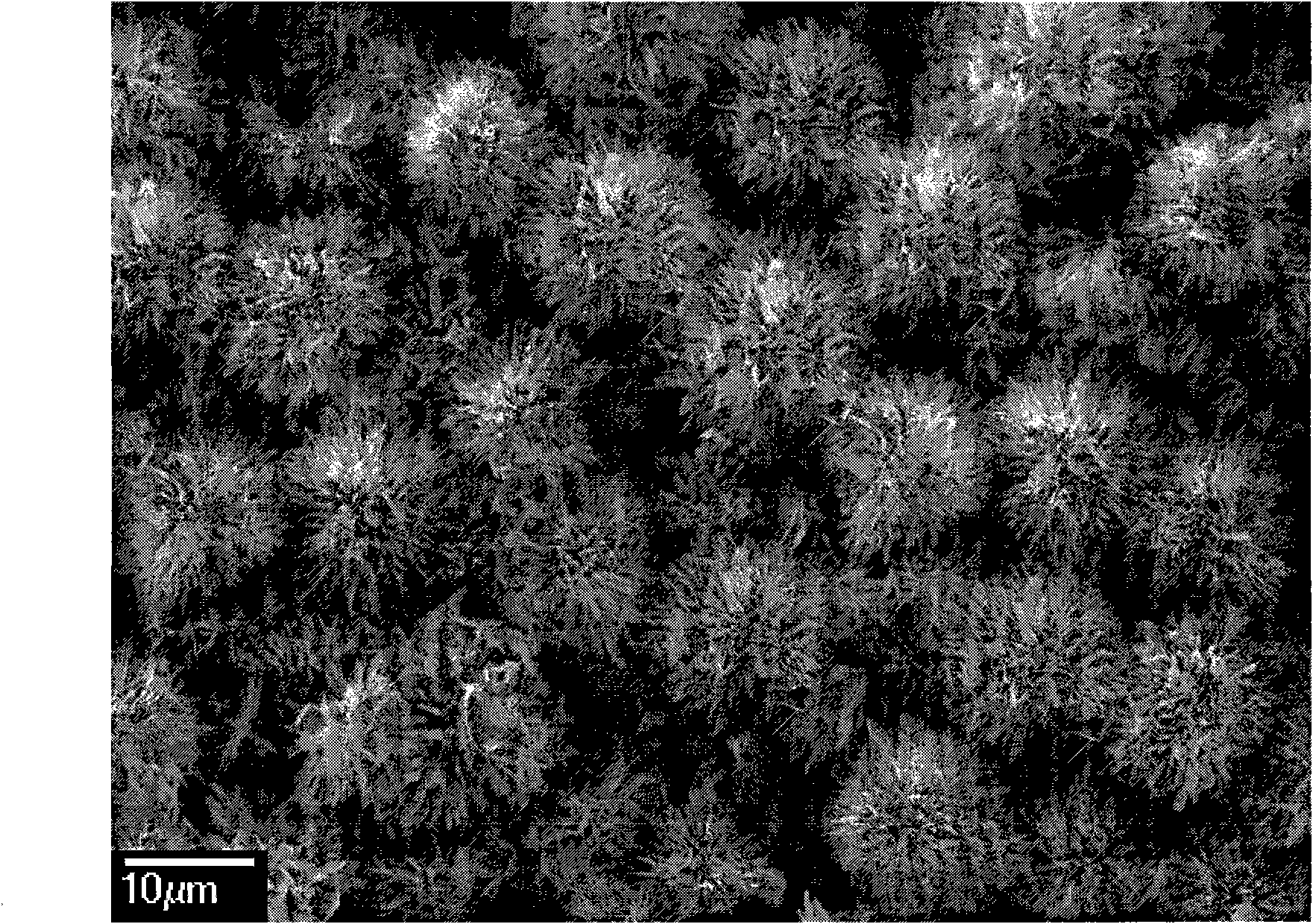
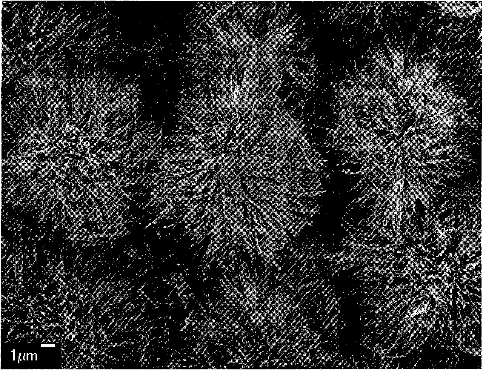
[0025] The VO 2 The crystal is ribbon VO 2 Nanoflower structure, oriented generation from nanoribbons, ribbon-like VO 2 The diameter of the nanoflower structure is 11um, and the width of the nanoribbon is 100nm.
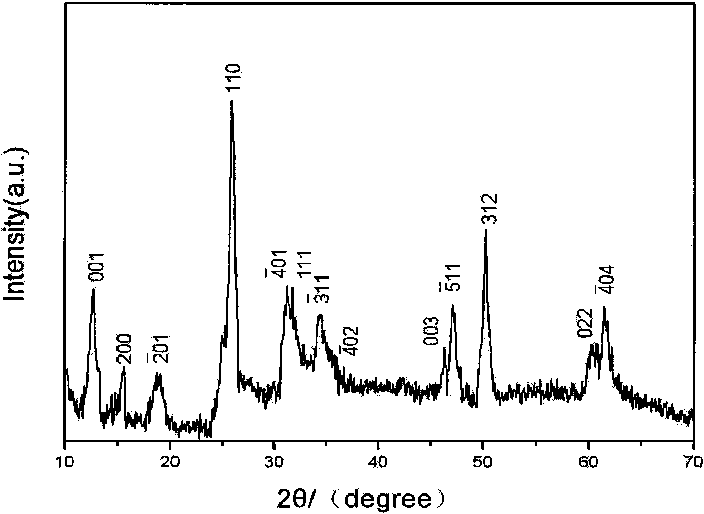
[0026] Ribbon VO 2 The X-ray diffraction pattern of the nanoflower structure is shown in figure 1 , banded VO 2 The SEM image of the nanoflower ...
Embodiment 2
[0028] (a) 0.4g oxalic acid (C 2 h 2 o 4 ) powder was dissolved in 40ml of water, stirred with a magnetic stirrer, after the powder was completely dissolved, 0.3g of ammonium metavanadate (NH 4 VO 3 ) powder, continue stirring to form an orange solution.
[0029] (b) Ribbon-shaped VO growth on silicon wafer 2 Nanoflower structure: first put the cleaned silicon wafer into an autoclave, then pour the above solution into a 50ml autoclave, seal the autoclave and put it into a blast drying oven, and keep the reaction at 160°C for 24 Hours, naturally cool down to room temperature, that is, the compound ribbon-shaped VO on the silicon wafer 2 Nanoflower-structured phase change materials.
[0030] The VO 2 The crystal is ribbon VO 2 Nanoflower structure, oriented generation from nanoribbons, ribbon-like VO 2 The diameter of the nanoflower structure is 12 μm, and the width of the nanoribbon is 200 nm.
[0031] Its X-ray diffraction pattern is basically similar to that of Exam...
Embodiment 3
[0033] (a) 0.45 oxalic acid (C 2 h 2 o 4 ) powder was dissolved in 40ml water, stirred with a magnetic stirrer, after the powder was completely dissolved, 0.5g ammonium metavanadate (NH 4 VO 3 ) powder, continue stirring to form a light yellow solution.
[0034] (b) Ribbon-shaped VO growth on silicon wafer 2 Nanoflower structure: first put the cleaned silicon wafer into an autoclave, then pour the above solution into a 50ml autoclave, seal the autoclave and put it into a blast drying oven, keep the reaction at 180°C for 36 Hours, naturally cool down to room temperature, that is, the compound ribbon-shaped VO on the silicon wafer 2 Nanoflower-structured phase change materials.
[0035] The VO 2 The crystal is ribbon VO 2 Nanoflower structure, oriented generation from nanoribbons, ribbon-like VO 2 The diameter of the nanoflower structure is 18 μm, and the width of the nanobelt is 700 nm.
[0036] Its X-ray diffraction pattern is basically similar to Embodiment 1, band-...
PUM
| Property | Measurement | Unit |
|---|---|---|
| diameter | aaaaa | aaaaa |
| concentration | aaaaa | aaaaa |
| width | aaaaa | aaaaa |
Abstract
Description
Claims
Application Information
 - R&D
- Intellectual Property
- Life Sciences
- Materials
- Tech Scout
- Unparalleled Data Quality
- Higher Quality Content
- 60% Fewer Hallucinations
Browse by: Latest US Patents, China's latest patents, Technical Efficacy Thesaurus, Application Domain, Technology Topic, Popular Technical Reports.
© 2025 PatSnap. All rights reserved.Legal|Privacy policy|Modern Slavery Act Transparency Statement|Sitemap|About US| Contact US: help@patsnap.com


