Ion implant method

A technology of ion implantation and ions, which is applied in the manufacture of electrical components, semiconductor/solid-state devices, circuits, etc., can solve problems such as threshold voltage inhomogeneity, components are difficult to meet specifications, and component characteristic drift, etc., to eliminate or reduce Adverse effects, effects of improving performance

Inactive Publication Date: 2010-11-24
SEMICONDUCTOR MANUFACTURING INTERNATIONAL (BEIJING) CORP
View PDF0 Cites 5 Cited by
  • Summary
  • Abstract
  • Description
  • Claims
  • Application Information

AI Technical Summary

Problems solved by technology

On the other hand, due to some damage to components during doping or ion implantation, there may be a transient enhanced diffusion of boron (boron) ions during heat treatment, resulting in a peak-shaped distribution of boron ions on both sides of the channel , so that the threshold voltage of the components increases with the decrease of the gate length (that is, the gate length), resulting in the non-uniformity of the threshold voltage distribution with the gate length, which is easy to cause the drift of the characteristics of the components. This effect is usually called Reverse Short Channel Effect (RSCE, Reverse Short Channel Effect)
[0004] Since the above-mentioned short channel effect and reverse short channel effect will adversely affect the performance of semiconductor components and increase the complexity of the processing process, it is difficult for the obtained components to meet the specifications required in the design, so The above two effects have become obstacles in the development of the manufacturing process of 65nm and below semiconductor components

Method used


Image

  • Ion implant method
  • Ion implant method
  • Ion implant method

Examples


Embodiment Construction

[0018] In order to make the object, technical solution and advantages of the present invention more clearly, the present invention will be further described in detail below in conjunction with the accompanying drawings and specific embodiments.

[0019] In the present invention, a method for ion implantation is proposed, which includes: performing ion implantation according to a pre-specified ion implantation sequence; the pre-specified ion implantation sequence is: germanium ions, arsenic ions, boron ions, indium ions, ions and carbon ions.

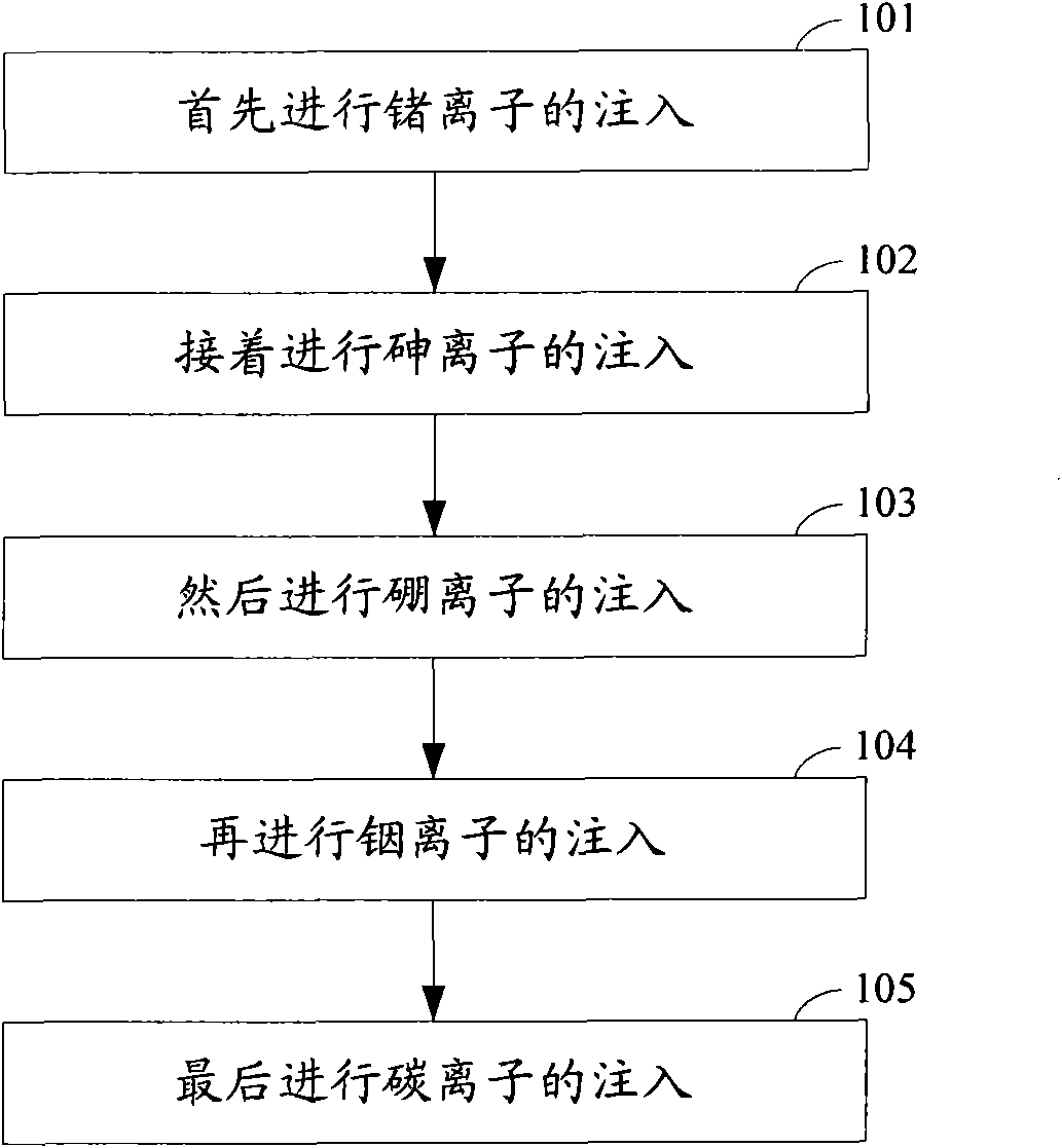
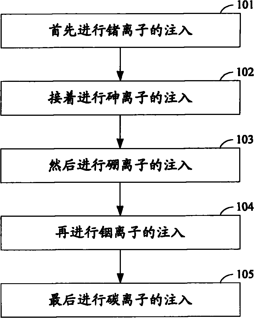
[0020] figure 1 It is a schematic flow chart of the ion implantation method in the present invention. Such as figure 1 As shown, in the ion implantation method provided in the present invention, the ion implantation can be performed according to the ion implantation sequence as follows:

[0021] In step 101, germanium (Ge) ions are implanted first.

[0022] In this step, the energy of the Ge ions may be 5-40Kev, and the dose may be 1...


PUM


Abstract

The invention discloses an ion implant method, comprising the following step: implanting ions according to the pre-specified ion implant sequence, wherein the sequence is as follow: germanium ions, arsenic ions, boron ions, indium ions and carbon ions. The method can effectively improve the performance of the semi-conductor components and eliminate or reduce the adverse impact of the short channel effect and / or reverse short channel effect on the semi-conductor components.

Description

technical field [0001] The invention relates to the manufacturing technology of semiconductor components, in particular to an ion implantation method. Background technique [0002] In the manufacturing technology of semiconductor components, since the conductivity of silicon in a pure state is very poor, only a small amount of impurities are added to silicon to change the structure and conductivity of silicon, so that silicon can become a useful semiconductor. The above process of adding a small amount of impurities to silicon is called doping. Silicon doping technology is the basis for preparing semiconductor components, and ion implantation (Ion Implant) technology is one of the most important doping methods. The ion implantation technique is a method of introducing a controllable amount of impurities into a silicon substrate, thereby changing its electrical properties. Since ion implantation technology can repeatedly control the concentration and depth of doped impuriti...

Claims


Application Information

Patent Timeline
Patent Type & Authority Applications(China)
IPC IPC(8): H01L21/265H01L21/335
Inventor 刘金华
Owner SEMICONDUCTOR MANUFACTURING INTERNATIONAL (BEIJING) CORP
Why Eureka
Try Eureka