High-performance glass encapsulation method of light emitting diode

A light-emitting diode and glass encapsulation technology, which is applied in electrical components, circuits, semiconductor devices, etc., can solve the problems of poor moisture resistance of organic matter, poor light transmission of lenses, and poor light transmission performance, so as to achieve anti-aging and simple and reliable process , low-cost effect

Inactive Publication Date: 2010-11-24
SOUTHEAST UNIV
View PDF5 Cites 5 Cited by
  • Summary
  • Abstract
  • Description
  • Claims
  • Application Information

AI Technical Summary

Problems solved by technology

Nowadays, transparent organic adhesives such as epoxy resin are widely used in the preparation of light-emitting diode (LED) lenses, but the lenses made of organic adhesives have poor light transmission and unstable properties. When heated, they will change color after working for a certain period of time. , the light transmission performance becomes poor, and the moisture resistance of organic matter is poor

Method used


Image

  • High-performance glass encapsulation method of light emitting diode
  • High-performance glass encapsulation method of light emitting diode
  • High-performance glass encapsulation method of light emitting diode

Examples


Embodiment 1

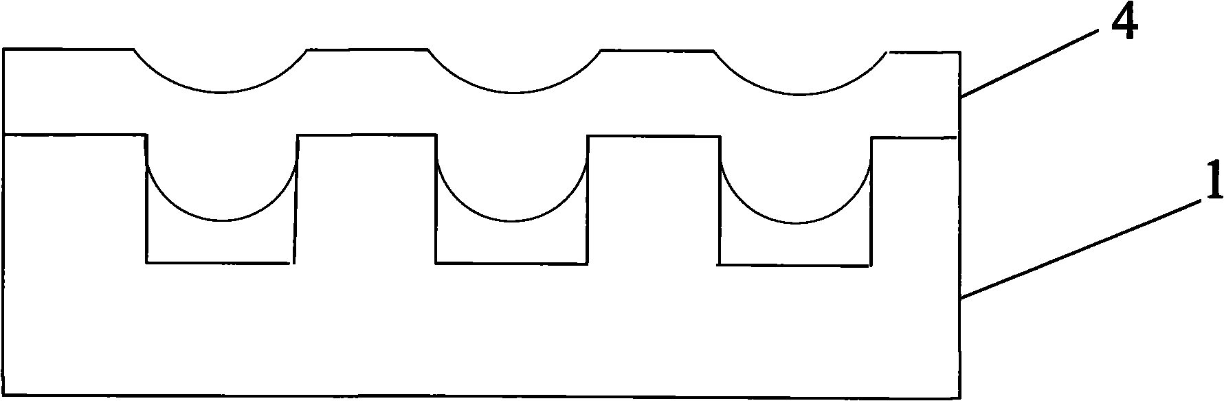
[0026]Embodiment 1 A high-performance glass packaging method for light-emitting diodes, comprising the following steps: the first step is to prepare a glass package with a microcavity on the back and a microlens on the front on a glass wafer; the glass package is heated by negative pressure. Forming method preparation, the specific preparation method can be seen in Example 3-4, its size is slightly larger than the light-emitting diode (LED) chip that needs to be packaged, the LED lead wire can be made according to the conventional process, the second step, the phosphor powder coating process: the fluorescent powder Powder (YAG: ce3+) mixed with silica gel (Jiuqi brand WH-7 type silicone sealant produced by Nanjing Helite Adhesive Co., Ltd.). The coverage area and thickness are determined, that is, the product of the area and the thickness is the volume to be coated and evenly coated on the surface of the LED chip to form a phosphor layer. The thickness can be selected according...

Embodiment 2

[0028] Embodiment 2 A high-performance glass encapsulation method for light-emitting diodes, comprising the following steps:

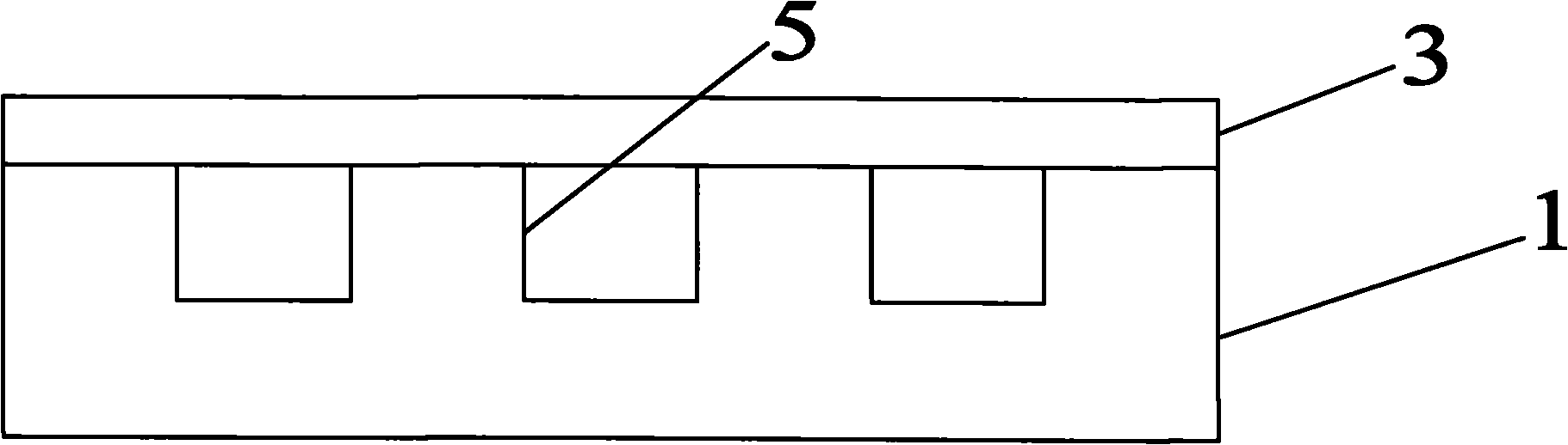
[0029] The first step is to prepare a glass lens array for sealing light-emitting diode (LED) chips on Pyrex7740 glass; when the glass is melted, it is sunken to the silicon microgroove to form a convex lens with a thick middle and thin surroundings, and a microcavity is formed under the lens at the same time, which can A light emitting diode (LED) chip is placed and sealed in the microcavity under the glass lens. For the preparation method of the glass lens microcavity, see the following embodiments of the present invention. The following examples of the present invention describe the method of making glass lenses by negative pressure forming. The glass microcavity prepared by the method described in the embodiment behind this embodiment adopts different microgroove aspect ratios, and the time and temperature of glass molding also adopt different val...

Embodiment 3

[0033] Embodiment 3 Manufacturing method of wafer-level glass lens microcavity

[0034] A method for manufacturing a wafer-level glass lens microcavity, comprising the following steps:

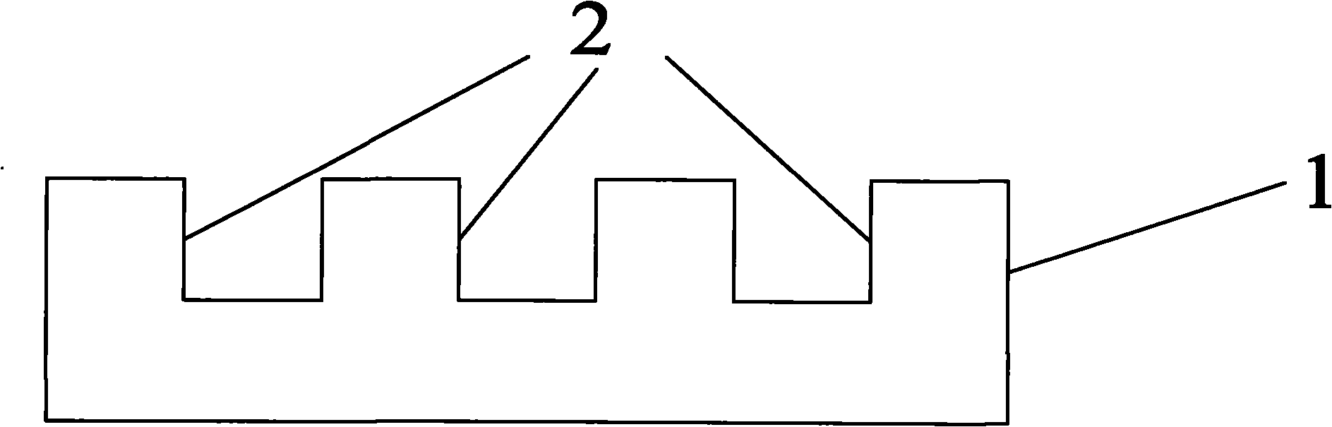
[0035] In the first step, a specific pattern is formed on an Si wafer (such as a 4-inch wafer) by etching using a Si micromachining process, and the micromachining process of the pattern structure on the Si wafer is a wet etching process or a dry inductively coupled plasma One of the bulk (ICP) etching process, reactive ion etching or deep reactive ion etching, the pattern can be a square or circular groove array, or a number of different graphics, (in fact, three-dimensionally, Engraving a specific pattern is to carve a groove on a silicon wafer, which is a pattern in two dimensions), and the aspect ratio of the microgroove can be less than 1:1 or greater than 1:1, for example: 2:1, 3:1, 4:1 , 7:1, 10:1, 15:1, 20:1, 25:1, the glass microcavity with high aspect ratio will provide more rheolog...


PUM


Abstract

The invention discloses a method for encapsulating a light emitting diode by using a glass lens cavity with high extracting rate and light beam collimation. The method comprises the following steps of: step 1, preparing a glass lens of a sealed light emitting diode chip on a glass wafer; step 2, coating fluorescent powder: evenly coating a fluorescent powder layer on the periphery of the light emitting diode chip or coating fluorescent powder on the glass inner wall; and step 3, filling silica gel in a gap between the light emitting diode chip and a glass ball cavity, splicing with the silicon wafer carried with the light emitting diode chip through a glass encapsulating body so that the light emitting diode chip is located in a cavity at the back side of the glass encapsulating body. The invention can realize white light emitting diode with even light intensity and has high emission rate of light rays; the encapsulation glass lens realizes the collimation of the light beam; the encapsulating reliability is very good; and the effective working time of the light emitting device is greatly prolonged.

Description

technical field [0001] The invention relates to a MEMS (micro-electro-mechanical system) packaging technology, in particular to a high-performance glass packaging method for a light-emitting diode. Background technique [0002] The development of white light-emitting diode (LED) technology has brought us into the fourth generation lighting era. White light-emitting diode (LED) lighting will surely replace today's lighting technology due to its advantages of low energy consumption and environmental protection. For lighting purposes, high-power white light-emitting diodes (LEDs) have been widely concerned by scientific research and enterprises. In order to generate sufficient light intensity, the working current of light-emitting diodes (LEDs) must be as large as possible, and the large working current is required for the packaging of light-emitting diodes (LEDs). The heat dissipation problem of the system has brought serious challenges. Therefore, by designing the optical p...

Claims


Application Information

Patent Timeline
Patent Type & Authority Applications(China)
IPC IPC(8): H01L33/48H01L33/50H01L33/56H01L33/58H01L33/62
Inventor 尚金堂徐超张迪陈波寅
Owner SOUTHEAST UNIV
Why Eureka
Try Eureka