
Semiconductor device manufacturing method, semiconductor device, electronic device, semiconductor manufacturing apparatus and storage medium

A manufacturing method and a technology for manufacturing a device, which are applied in the field of storage media and can solve problems such as increased wiring resistance and lack of reactivity

Inactive Publication Date: 2010-11-24
TOKYO ELECTRON LTD +1
View PDF3 Cites 3 Cited by
  • Summary
  • Abstract
  • Description
  • Claims
  • Application Information

AI Technical Summary

Problems solved by technology

This manganese oxide is an insulator, which causes a large increase in wiring resistance, and because it is passive, it lacks reactivity, and additional steps such as punching are required to remove it.

Method used


Image

  • Semiconductor device manufacturing method, semiconductor device, electronic device, semiconductor manufacturing apparatus and storage medium
  • Semiconductor device manufacturing method, semiconductor device, electronic device, semiconductor manufacturing apparatus and storage medium
  • Semiconductor device manufacturing method, semiconductor device, electronic device, semiconductor manufacturing apparatus and storage medium

Examples


Embodiment

[0154] Next, experiments performed on the present invention will be described. In the experiment, used Figure 8 (a) Wafer W for testing is shown. This wafer W was produced as follows. First, a film was formed on a silicon substrate 90 by a plasma CVD method using TEOS (Tetra Ethoxy Silane, alias Tetraethyl Orthosilicate) at 350° C. to obtain a silicon oxide film 91 with a film thickness of 100 nm. Then, on this silicon oxide film 91, a manganese oxide layer 92 is formed in the Cu-MnOxCVD module 5 described above under the following film formation conditions. In addition, on the surface of the wafer W, a copper film 93 was formed by a sputtering method so as to have a film thickness of 100 nm. Thereafter, the wafer W was heat-treated under the following annealing conditions in order to confirm the presence or absence of copper diffusion. Thereafter, the experiments described below were performed on the wafer W. Also, since this experiment does not require good step covera...


PUM

PropertyMeasurementUnit
coating thicknessaaaaaaaaaa

Abstract

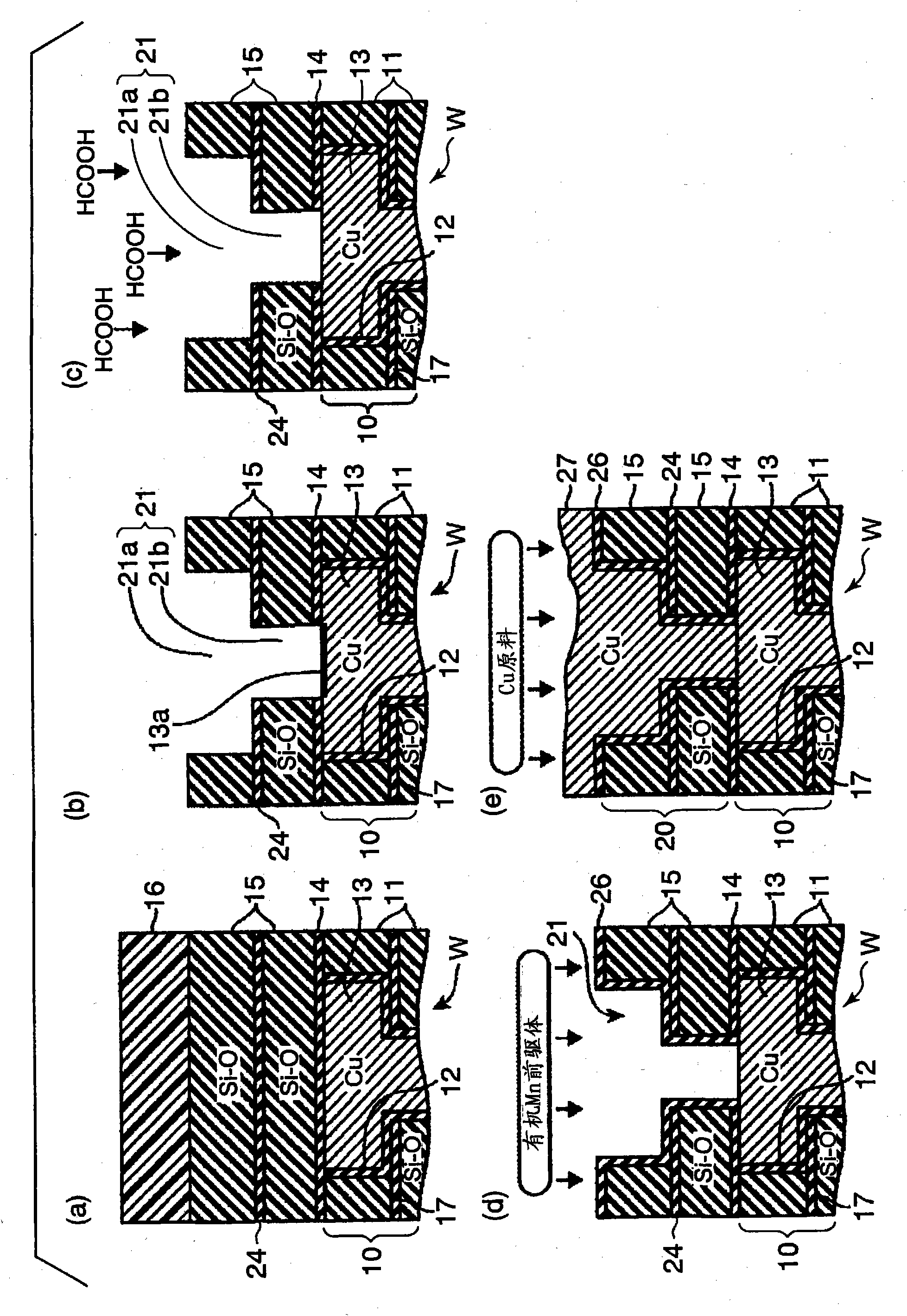
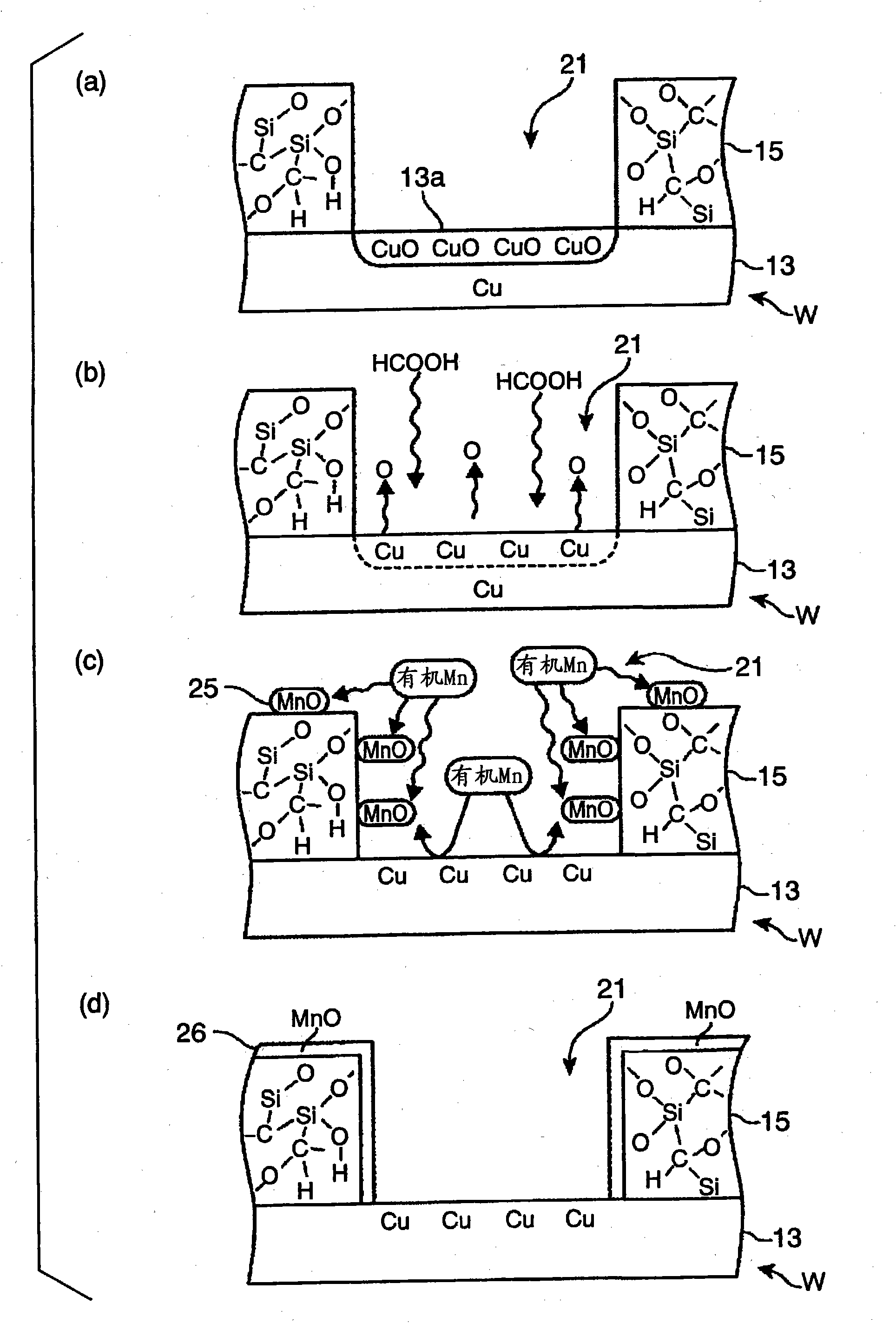
A barrier film having excellent step coverage is formed, and furthermore, increase of wiring resistance is suppressed, at the time of forming the barrier film on an exposed surface of an interlayer insulating film, which is on a substrate and has a recessed section formed thereon, and forming copper wiring electrically connected to metal wiring on a lower layer side in the recessed section. An oxide film on a surface of the copper wiring which is on the lower layer side and exposed from the bottom surface of the recessed section formed on the interlayer insulating film is reduced or etched and oxygen on the surface of the copper wiring is removed. Then, manganese oxide, i.e., a self-formed barrier layer, is selectively grown on an oxygen containing portion, such as the side walls of the recessed section and a surface of the interlayer insulating film by supplying an organic metal compound which contains manganese but no oxygen, while the manganese oxide is prevented from growing on the surface of the copper wiring. Then, the recessed section is filled with copper.

Description

technical field [0001] The present invention relates to a method of manufacturing a semiconductor device in which copper is embedded in a concave portion formed in an interlayer insulating film to form copper wiring, a semiconductor device manufactured by the method, an electronic device including the semiconductor device, a semiconductor manufacturing device, and the method stored therein storage medium. Background technique [0002] The multilayer wiring structure of a semiconductor device is formed by embedding metal wiring into an interlayer insulating film. As the material of the metal wiring, copper (Cu) is used because of its small electromigration and low resistance. Technology, commonly used is the mosaic (damascene) process. In addition, as the interlayer insulating film, a low dielectric constant material is used, for example, a film composed of a silicon compound containing silicon (Si) and oxygen (O) or carbon (C), such as SiO, SiOF, SiC, SiOC, SiCOH , SiCN, p...

Claims


Application Information

Patent Timeline
Patent Type & Authority Applications(China)
IPC IPC(8): H01L21/768C23C16/40H01L21/285
CPCH01L21/76814C23C28/345C23C28/00H01L21/28562C23C16/40C23C28/322H01L21/76844C23C28/04H01L21/76831
Inventor 松本贤治伊藤仁佐藤浩小池淳一根石浩司
Owner TOKYO ELECTRON LTD
Learn More