

Manufacture method of bi-distributed feedback laser double-amplifier based on gamma waveguide
A manufacturing method and double-distribution technology, applied in the direction of semiconductor lasers, semiconductor laser devices, lasers, etc., can solve problems such as the inability to take into account the depth of signal modulation and the reduction of signal tuning range
- Summary
- Abstract
- Description
- Claims
- Application Information
AI Technical Summary
Problems solved by technology
Method used
Image

Examples
Embodiment
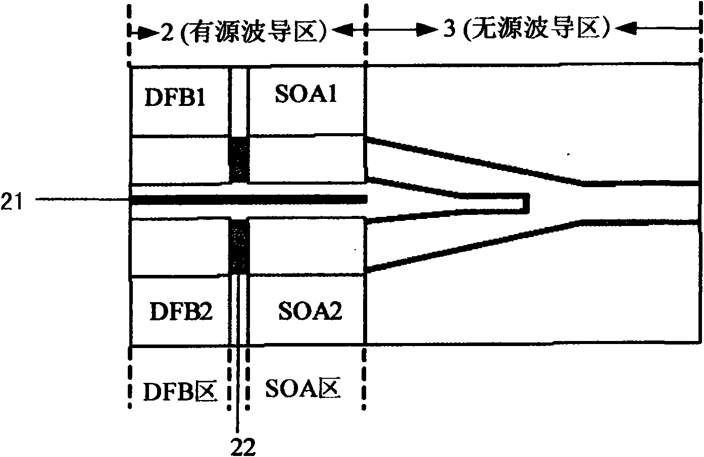
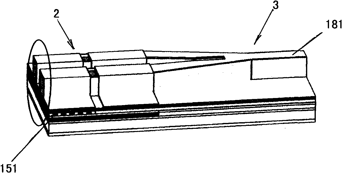
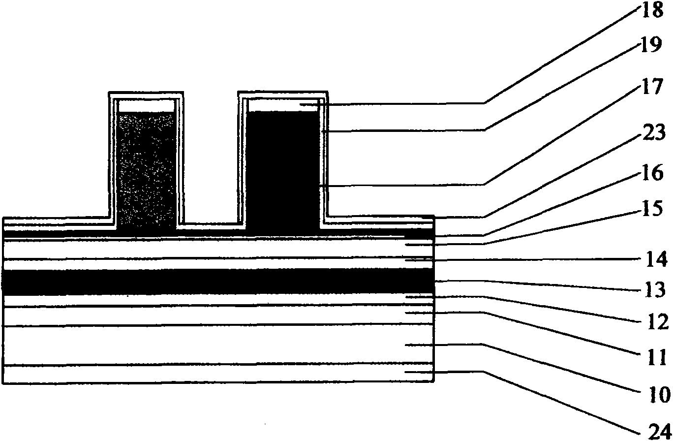
[0037] please refer again figure 1 , figure 2 , image 3 with Figure 4 A kind of manufacturing method based on Y waveguide double distributed feedback laser+double amplifier provided by the present invention, comprises following manufacturing steps:
[0038] Step 1: Select an N-type indium phosphide substrate 10;
[0039] Step 2: On the N-type indium phosphide substrate 10, sequentially epitaxially fabricate an InP buffer layer 11 of 1.5 μm, a lower waveguide layer 12 of 100 nm, a multi-quantum well active region 13, an upper waveguide layer 14 of 100 nm and a grating layer 15, Forming a material structure; wherein the multi-quantum well active region 13 is an InGaAsP material, the bandgap wavelength of the material is 1.55 μm, the number of quantum wells is 6, and the total thickness is 90 nanometers;
[0040] Step 3: Fabricate the passive waveguide region 3 on one side of the material structure, and the active waveguide region 2 on the other side; when making the passi...
PUM
 Abstract
Description
Claims
Application Information