
Etchant composition for and etching method of materials containing copper

A technology of etchant and composition, which is applied in the etchant composition for copper-containing materials and the field of etching of copper-containing materials, and can solve the problems of inability to obtain etching performance, poor shape of circuit patterns, etc.

Inactive Publication Date: 2011-01-19
ADEKA CORP
View PDF4 Cites 11 Cited by
  • Summary
  • Abstract
  • Description
  • Claims
  • Application Information

AI Technical Summary

Problems solved by technology

[0010] However, the etchant compositions disclosed in Patent Documents 1 and 2 have a problem in that etching performance sufficient for fine circuits cannot be obtained.
Especially in the case of forming a pattern with a narrow etching space (line spacing, gap) of removed copper (for example, 10 μm to 60 μm), the shape of the circuit pattern will be defective.

Method used


Image

  • Etchant composition for and etching method of materials containing copper
  • Etchant composition for and etching method of materials containing copper
  • Etchant composition for and etching method of materials containing copper

Examples


Embodiment 1 and comparative example 1

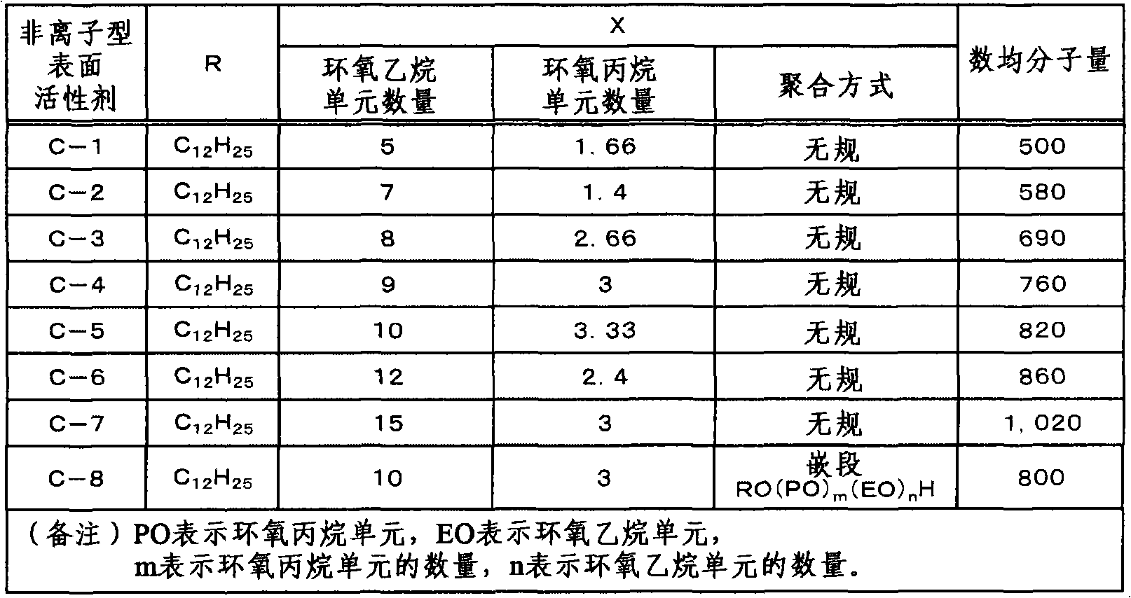
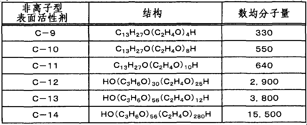
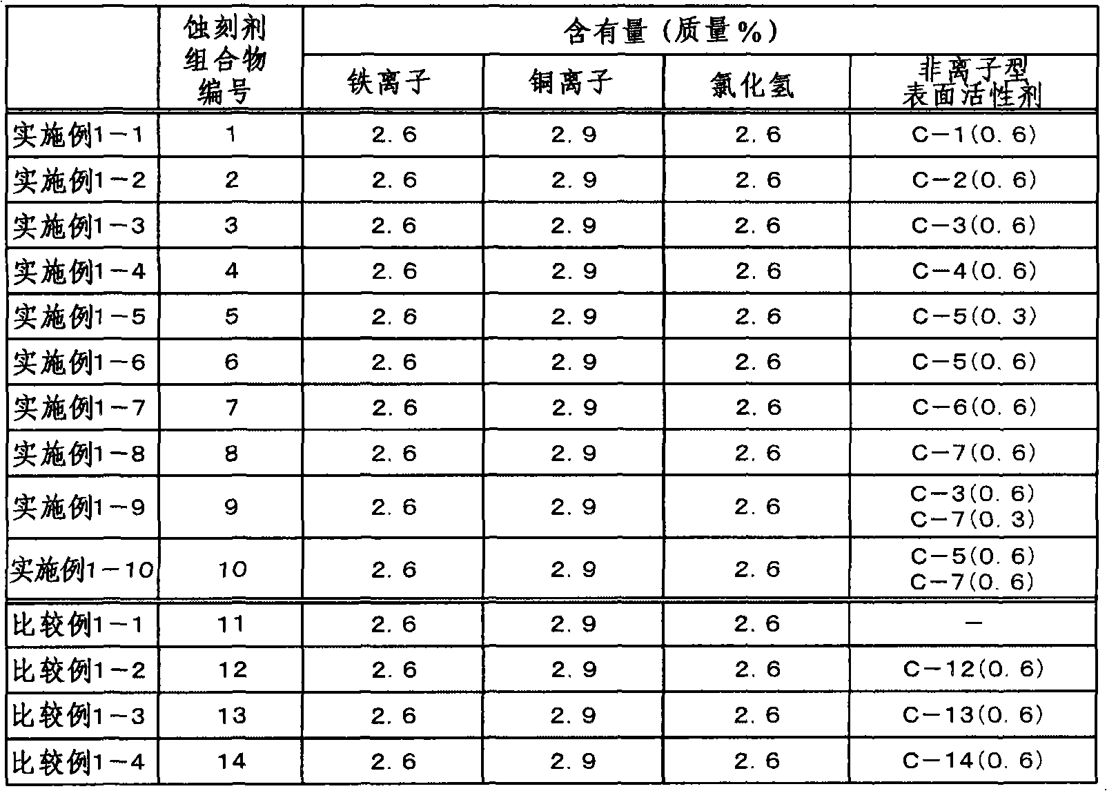
[0068] The nonionic surfactant shown in Table 1 and Table 2, ferric chloride (iron ion), hydrogen chloride, copper (copper ion) and water were mixed according to the composition in Table 3 to obtain an etchant composition. In addition, the remainder of the content in Table 3 is water.

[0069] table 3

[0070]

Embodiment 2 and comparative example 2

[0072] The etchant obtained in the above-mentioned Examples and Comparative Examples was used for a test substrate in which a dry film resist patterned with a line width of 100 μm and a predetermined line spacing (etching space) was formed on a resin substrate having a copper foil with a thickness of 20 μm. composition, spray etching the test substrate under specified conditions. Thereafter, the dry film resist was removed by immersing in a 5% by mass sodium hydroxide aqueous solution (50° C.) for 1 minute. The shape of the obtained copper circuit was evaluated as follows.

[0073] (1) Wiring upper width (top width)

[0074] The cross section (observation section) was measured with an optical microscope. The unit is μm.

[0075] (2) Wiring lower part width (bottom width)

[0076] The cross section (observation section) was measured with an optical microscope. The unit is μm.

[0077] (3) Difference between bottom width and top width

[0078] Calculate it using the follo...

Embodiment 3 and comparative example 3

[0088] The nonionic surfactants shown in Table 1 and Table 2, ferric chloride, hydrogen chloride, copper, and water were mixed according to the composition in Table 6 to obtain an etchant composition. In addition, the remainder of the content in Table 6 is water.

[0089] Table 6

[0090]


PUM


Abstract

The invention provides an etchant composition for materials containing copper capable of forming micro circuit patterns without bad shapes and an etching method of materials containing copper. The etchant composition for materials containing copper is composed of aqueous solution which comprises (A) at least one 0.1-15% by mass oxidant component selected from copper ion and iron ion, (B) 0.1-20% by mass hydrogen chloride, and (C) 0.001-5% by mass non-ionic surfactant which is shown in the following formula (1) and has 1,500-3,000 number-average molar mass. In the formula (1), R represents alkyl having 8-18 carbon atoms; X represents polypropylene alkyl which is formed by the irregular polymerization or block polymerization of ethylene oxide unit and propylene epoxide. The formula (1) is R-O-X-H.

Description

technical field [0001] The present invention relates to an etchant composition for a copper-containing material and an etching method for a copper-containing material, and specifically relates to an etchant composition for a copper-containing material and an etching method for a copper-containing material capable of forming a fine circuit pattern (circuit wiring) without shape defects etching method. Background technique [0002] A printed wiring board (or film) on which circuit wiring is formed on the surface is widely used for mounting electronic parts, semiconductor elements, and the like. Furthermore, in recent years, along with demands for miniaturization and higher functionality of electronic equipment, higher density and thinner circuit wiring of printed wiring boards (or films) are also expected. [0003] As a method for producing high-density circuit wiring, there are known methods called a subtractive method (subtractive method) and a semi-additive method (semi-ad...

Claims


Application Information

Patent Timeline
IPC IPC(8): C23F1/18C23F1/02
CPCC23F1/02C23F1/18H05K3/06H05K3/062
Inventor 正元祐次下泽正和
Owner ADEKA CORP
Learn More