Panel display driving chip based on silicon on insulator (SOI) and preparation method thereof

A flat-panel display and driver chip technology, applied in semiconductor/solid-state device manufacturing, electric solid-state devices, semiconductor devices, etc., can solve the problems of high process conditions, waste of chip area, insufficient reliability, etc., and achieve good anti-latch performance. , The effect of excellent reliability and low power consumption

Inactive Publication Date: 2011-02-02
SOUTHEAST UNIV
View PDF0 Cites 10 Cited by
  • Summary
  • Abstract
  • Description
  • Claims
  • Application Information

AI Technical Summary

Problems solved by technology

At present, the lateral double-diffused metal oxide semiconductor tube is mainly used as the output high-voltage device of the commonly used plasma flat panel display driver chip, and the lateral double-diffused metal oxide semiconductor tube is limited by its working principle, and it must occupy a large chip as a high-voltage output device. Area, and with the development of lateral insulated gate bipolar transistors, it has begun to gradually replace the application of lateral double-diffused metal oxide semiconductor transistors to achieve smaller chip areas and lower power consumption; the main isolation structures include: single slot Filling silicon dioxide and polysilicon isolation, deep junction isolation and pn junction self-isolation, however, the single-slot isolation structure requires high process conditions and insufficient reliability. The chip area is wasted by the pn junction isolation high-voltage structure, and the area of ​​the chip used for isolation exceeds 20%, with the advancement of silicon-on-insulator (SOI) technology, the use of double-groove isolation structures can not only ensure the reliability of isolation, but also effectively improve chip utilization. The isolation structure occupies less than 5% of the chip area

Method used


Image

  • Panel display driving chip based on silicon on insulator (SOI) and preparation method thereof
  • Panel display driving chip based on silicon on insulator (SOI) and preparation method thereof
  • Panel display driving chip based on silicon on insulator (SOI) and preparation method thereof

Examples


Embodiment 1

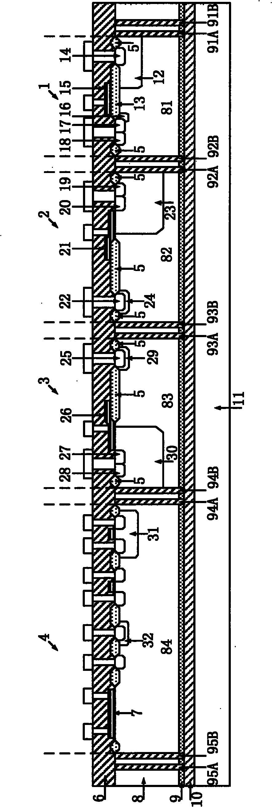
[0021] Below in conjunction with accompanying drawing, the present invention is described in detail, as figure 1Shown, a kind of flat panel display drive chip comprises P-type substrate 11, is provided with buried oxide layer 10 on P-type substrate 11, is characterized in that is provided with N-type buried layer 9 on buried oxide layer 10, in N The buried layer 9 is provided with a high-voltage P-type lateral metal oxide semiconductor transistor 1, a high-voltage N-type lateral metal oxide semiconductor transistor 2, a high-voltage N-type lateral insulated gate bipolar transistor 3, and a low-voltage device 4. The oxide semiconductor transistor 1 is adjacent to the high-voltage N-type lateral metal-oxide-semiconductor transistor 2 and the drain end of the high-voltage P-type lateral metal-oxide semiconductor transistor 1 is adjacent to the source end of the high-voltage N-type lateral metal-oxide semiconductor transistor 2. The N-type lateral insulated gate bipolar transistor...

Embodiment 2

[0030] The preparation method of the high-voltage device for driving the flat panel display of the present invention is:

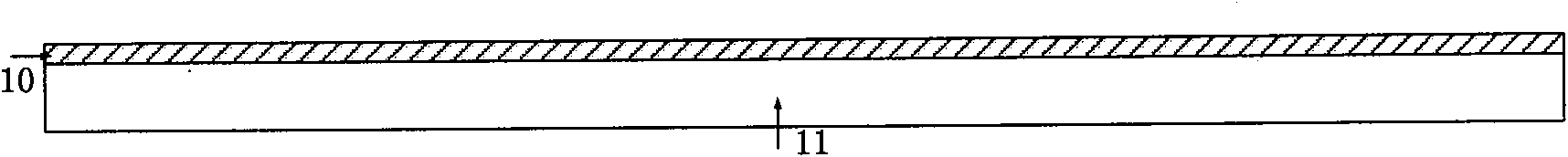
[0031] The first step: take the impurity concentration as 1.0e15cm -3 The P-type substrate 11 shown in Figure 2(a) is pre-cleaned; the buried oxide layer 10 is prepared on the P-type substrate 11 as shown in Figure 2(b); then the growth impurity concentration is 1.5e15cm -3 N-type epitaxial layer 8, and pass a dose of 1e12cm -2 As shown in Figure 2 (c), an N-type buried layer 9 is fabricated on the N-type epitaxial layer 8; a P-type body of a high-voltage N-type lateral metal oxide semiconductor transistor 2 is respectively fabricated on the N-type epitaxial layer 8 Region 23 and the P-type body region 30 of the high-voltage N-type lateral insulated gate bipolar transistor 3 are shown in Figure 2(d); then the P-type drift region 12 fabricated on the N-type epitaxial layer 8 is shown in Figure 2(e) As shown; Next, on the N-type epitaxial layer 8, the drai...


PUM


Abstract

The invention provides a panel display driving chip based on a silicon on insulator (SOI) material, which is composed of a high-voltage P-type transverse metal oxide transistor, a high-voltage N-type transverse metal oxide transistor, a high-voltage N-type transverse insulated gate bipolar transistor and a low-voltage device, wherein each high-voltage device is isolated by a double-groove structure filled with silicon dioxide, which starts from the oxygen buried layer and ends at the field oxide on the device surface via the N-type buried layer and the N-type epitaxial layer; and the connection region of the epitaxial layer and the oxygen buried layer is provided with the N-type buried layer. The preparation method comprises the following steps: making the oxygen buried layer, the N-type buried layer and the deposition epitaxial layer on the P-type substrate; making the high-voltage P wells of the high-voltage N-type transverse metal oxide transistor and the high-voltage N-type transverse insulated gate bipolar transistor, the P-type drift region of the high-voltage P-type transverse metal oxide transistor, the buffer layer of the high-voltage transistor, the low-voltage well of the low-voltage transistor, the source and drain regions and the contact holes; and evaporating aluminium, photoetching aluminium in a reversed mode, forming electrodes and metal field plates, and passivating.

Description

technical field [0001] The invention relates to a flat panel display drive chip and a preparation method thereof, and is especially suitable for a row address selection drive chip and a column address selection drive chip for a plasma flat panel display (PDP). Background technique [0002] On the whole, the plasma flat panel display driver chip is mainly composed of a low-voltage logic circuit controlling a high-voltage output circuit. With the continuous improvement of display technology and drive technology, plasma flat panel display driver chips have the following development trends: higher operating frequency, smaller size of high-voltage devices, lower power consumption, and better performance. This has increasingly stringent requirements on the output stage high-voltage power devices of the driver chip. At present, the lateral double-diffused metal oxide semiconductor tube is mainly used as the output high-voltage device of the commonly used plasma flat panel display ...

Claims


Application Information

Patent Timeline
Patent Type & Authority Applications(China)
IPC IPC(8): H01L21/762H01L27/06H01L29/06H01L29/78
Inventor 钱钦松庄华龙孙伟锋吴虹陆生礼时龙兴
Owner SOUTHEAST UNIV
Why Eureka
Try Eureka