Quasi one-dimensional nano structural thermoelectric material, device and preparation method thereof

A technology of thermoelectric materials and nanostructures, which is applied in the manufacture/processing of thermoelectric devices, parts and components of thermoelectric devices, etc., can solve the problems of no thermoelectric devices, achieve increased scattering, good thermal stability, and facilitate mass production and application Effect

Inactive Publication Date: 2011-02-09
SUN YAT SEN UNIV
View PDF9 Cites 26 Cited by
  • Summary
  • Abstract
  • Description
  • Claims
  • Application Information

AI Technical Summary

Problems solved by technology

Although there are a large number of literature reports on the application of electrochemical methods to grow thermoelectric material nanowires of various compositions in the holes of alumina or polymer nano-templates, and the...

Method used


Image

  • Quasi one-dimensional nano structural thermoelectric material, device and preparation method thereof
  • Quasi one-dimensional nano structural thermoelectric material, device and preparation method thereof
  • Quasi one-dimensional nano structural thermoelectric material, device and preparation method thereof

Examples


Embodiment 1

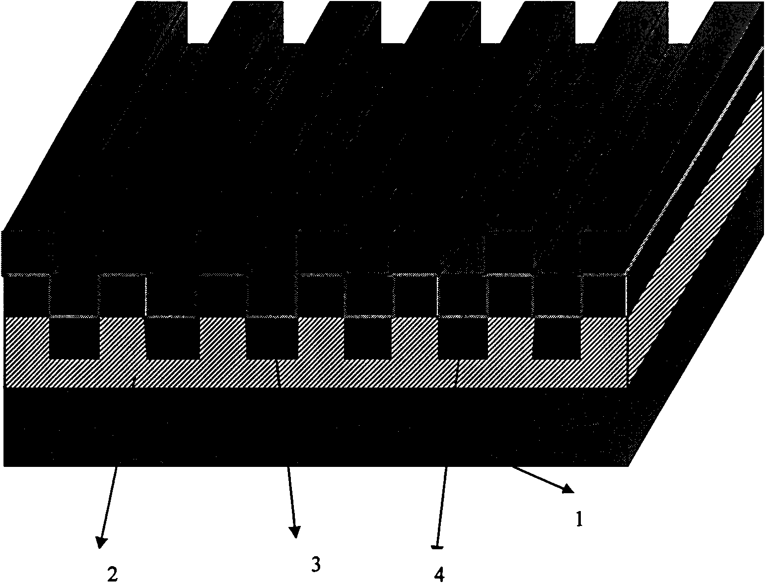
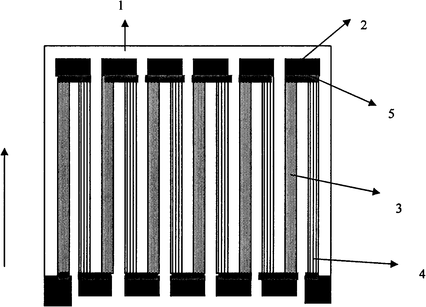
[0045] In this example, p-type and n-type Bi 2 Te 3 As a thermoelectric material, the thermoelectric layer doped with W particles is used as a phonon scattering layer, magnetron sputtering is used as a deposition method, and ultraviolet nanoimprinting technology is used as a method for preparing a grooved substrate, and the substrate is made of glass.

[0046] Specific steps are as follows:

[0047] (1) Apply embossing glue on a glass sheet (1cm×1cm) that has been ultrasonically cleaned by 1mol / L NaOH, 1mol / L Hcl solution, anhydrous ethanol, and deionized water, and the rectangular groove A template (20nm x 20nm in cross-section) is pressed on top, allowing UV light to pass through the template to cure the polymer. The template is separated from the substrate, and the residual polymer layer is removed to obtain a substrate with grooves (20nm×20nm).

[0048] (2) Place the substrate on the rotating substrate holder of the magnetron sputtering instrument, and install the p...

Embodiment 2

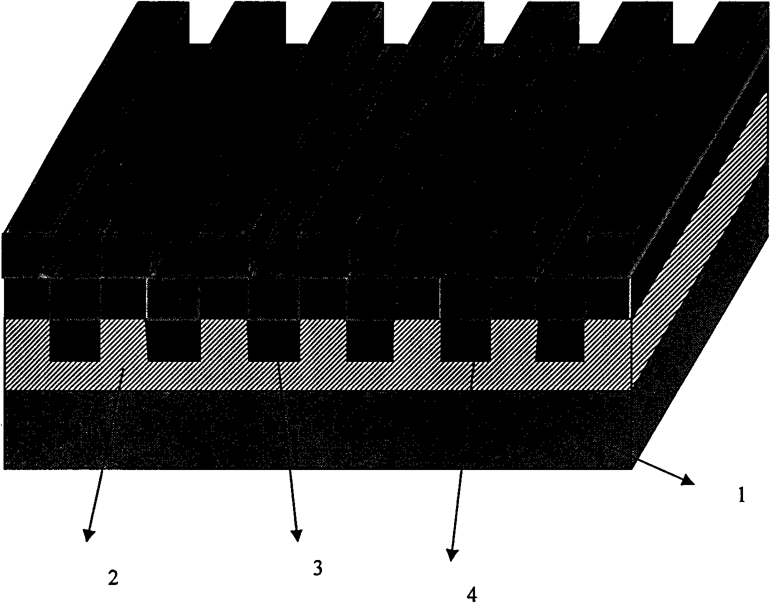
[0056] In this example, p-type and n-type PbTe were selected as the thermoelectric material, the thermoelectric layer doped with SiO2 particles was used as the phonon scattering layer, the magnetron sputtering was used as the deposition method, and the ultraviolet nanoimprinting technology was used as the method for preparing the trench substrate. Means, the substrate uses mica.

[0057] Specific steps are as follows:

[0058](1) Apply embossing glue on the newly dissected mica sheet (1cm×1cm) that has been ultrasonically cleaned by 1mol / L NaOH, 1mol / L HCl solution, absolute ethanol, and deionized water. A template with rectangular grooves (5nm x 5nm) was pressed on top, allowing UV light to pass through the template to cure the polymer. The template is separated from the substrate, and the residual polymer layer is removed to obtain a substrate with grooves (5nm×5nm).

[0059] (2) Place the substrate on the rotating substrate holder of the magnetron sputtering instrumen...

Embodiment 3

[0067] In this example, p-type and n-type Bi 2 Te 3 As a thermoelectric material, SiO 2 As a continuous layer of insulating material. Magnetron sputtering is used as a deposition method, and ultraviolet nanoimprint technology is used as a method for preparing grooved substrates, and silicon oxide wafers are used as substrates.

[0068] Specific steps are as follows:

[0069] (1) Take a silicon wafer (1cm×1cm), oxidize it, and then use 1mol / L NaOH, 1mol / L Hcl solution, absolute ethanol, and deionized water to clean it ultrasonically, and then apply the imprinting glue. A template with rectangular grooves (200nm x 200nm) was pressed onto it, allowing UV light to pass through the template to cure the polymer. The template is separated from the substrate, and the residual polymer layer is removed to obtain a substrate with grooves (200nm×200nm).

[0070] (2) Place the substrate on the rotating substrate holder of the magnetron sputtering instrument, install the Bi 2 Te ...


PUM

PropertyMeasurementUnit
Thicknessaaaaaaaaaa
Thicknessaaaaaaaaaa
Granularityaaaaaaaaaa

Abstract

The invention discloses a quasi one-dimensional nano structural thermoelectric material, a device and a preparation method thereof. The thermoelectric material comprises an insulating substrate, at least two thermoelectric material layers ant at least two phonon scattering layers; parallel nano grooves arranged periodically are distributed on the surface of the insulating substrate, and the cross sections of the grooves have rectangular fluctuated structures; the thermoelectric material layers are covered on the surface of the substrate, and the cross sections of the thermoelectric material layers have rectangular fluctuated periodical structures; and the thermoelectric material layers and the phonon scattering layers are alternately covered in rectangular fluctuated periodical structures. The size of the nano wire cross section can be controlled by changing the size of the substrate grooves and the deposition time, the scattering of phonons transmitted along the nano wire direction can be increased by changing the nano wire cross section area and the interface between the nano wires, the thermal conductivity of the material can be reduced, and the thermoelectric conversion efficiency of the material can be improved; and the prepared device has high thermoelectric conversion efficiency and good thermal stability.

Description

technical field [0001] The invention belongs to the field of thermoelectric materials, relates to a thermoelectric material, a device and a preparation method thereof, in particular to a quasi-one-dimensional nanometer material and a device which have high thermoelectric conversion efficiency and can be made into a thermoelectric device whose thermoelectric transmission is not limited by the thickness of the material and its preparation method. Background technique [0002] Thermoelectric materials and devices are materials and devices that can directly convert heat and energy as well as electricity and heat. Improving the conversion efficiency of thermoelectric materials has always been the central task in this field, that is, the dimensionless performance index ZT value that determines the conversion efficiency. Improve (ZT=a 2 σT / k, where a is the Seebeck coefficient, σ is the electrical conductivity, k is the thermal conductivity, and T is the absolute temperature. The...

Claims


Application Information

Patent Timeline
IPC IPC(8): H01L35/02H01L35/34
Inventor 任山李立强叶志超李义兵洪澜
Owner SUN YAT SEN UNIV
Why Eureka
Try Eureka