Manufacturing method of back passivation cell
A manufacturing method and technology of back passivation, applied in final product manufacturing, sustainable manufacturing/processing, circuits, etc., can solve the problems of limited utilization of long-wavelength photons and solar energy conversion efficiency, and achieve superior front passivation and back surface passivation. Passivation performance, good reflection effect, good photoelectric response effect
- Summary
- Abstract
- Description
- Claims
- Application Information
AI Technical Summary
Problems solved by technology
Method used
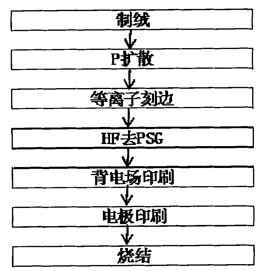
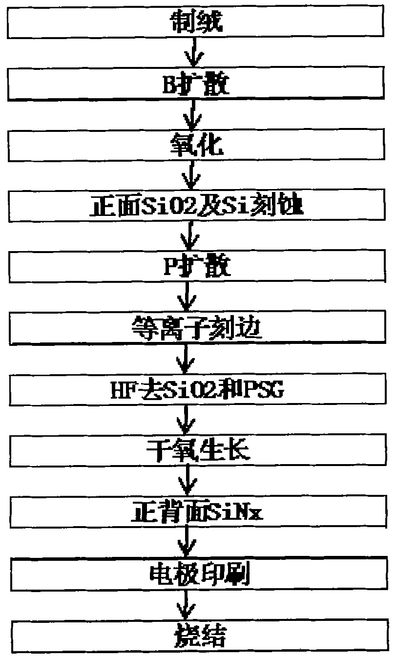
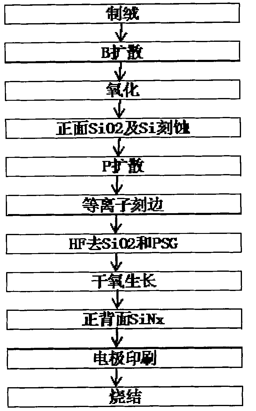
Image

Examples
Embodiment 1
[0023] The operation steps are as follows:
[0024] a. Select P-type monocrystalline silicon wafers, crystal plane (100), doping concentration 0.5Ωcm, perform routine cleaning after slicing, and texture the surface;
[0025] b. Put the textured silicon wafer into the B diffusion tube for diffusion. The temperature of the diffusion is 900°C, and the diffusion square resistance is 70Ω;
[0026] c. Put into the oxidation furnace to grow wet oxygen, thermally grown SiO 2 The film thickness is 80nm, and the oxidation temperature is 900°C;
[0027] d. Use NH as the main component 4 The etching slurry of HF etches the front side of the silicon wafer for 15 minutes to etch away the SiO 2 and Si in the B diffusion junction, keep the SiO on the back side 2 The presence of, and then use ionized water plus ultrasonic cleaning silicon wafer;
[0028] e. Put the silicon wafer into P diffusion for diffusion, the diffusion temperature is 830°C, and the diffusion square resistance is 60Ω;...
Embodiment 2
[0036] The operation steps are as follows:
[0037] a. Select P-type monocrystalline silicon wafers, crystal plane (100), doping concentration 2.5Ωcm, routine cleaning after slicing, and surface texture;
[0038] b. Put the textured silicon wafer into the B diffusion tube for diffusion. The temperature of the diffusion is 950°C, and the diffusion square resistance is 40Ω;
[0039] c. Put into the oxidation furnace to grow wet oxygen, thermally grown SiO 2 The film thickness is 120nm, and the oxidation temperature is 950°C;
[0040] d. Use NH as the main component 4 The etching slurry of HF etches the front side of the silicon wafer for 25 minutes to etch away SiO2 and Si in the B diffusion junction, and keep the SiO2 on the back side. 2 The presence of, and then use ionized water plus ultrasonic cleaning silicon wafer;
[0041] e. Put the silicon wafer into P diffusion for diffusion, the diffusion temperature is 850°C, and the diffusion resistance is 70Ω;
[0042] f. Plas...
PUM
| Property | Measurement | Unit |
|---|---|---|
| electrical resistance | aaaaa | aaaaa |
Abstract
Description
Claims
Application Information
 - R&D
- Intellectual Property
- Life Sciences
- Materials
- Tech Scout
- Unparalleled Data Quality
- Higher Quality Content
- 60% Fewer Hallucinations
Browse by: Latest US Patents, China's latest patents, Technical Efficacy Thesaurus, Application Domain, Technology Topic, Popular Technical Reports.
© 2025 PatSnap. All rights reserved.Legal|Privacy policy|Modern Slavery Act Transparency Statement|Sitemap|About US| Contact US: help@patsnap.com